THAT — The Analog Thing · Volume 8
THE Analog Thing — Volume 8 — Cheatsheet (field-grade)
Field-ready reference panels distilling Vols 1–7: jack colors, element counts, scaling algebra, patch recipes, mode sequences, daisy-chain wiring, and the full spec card — all on one bench
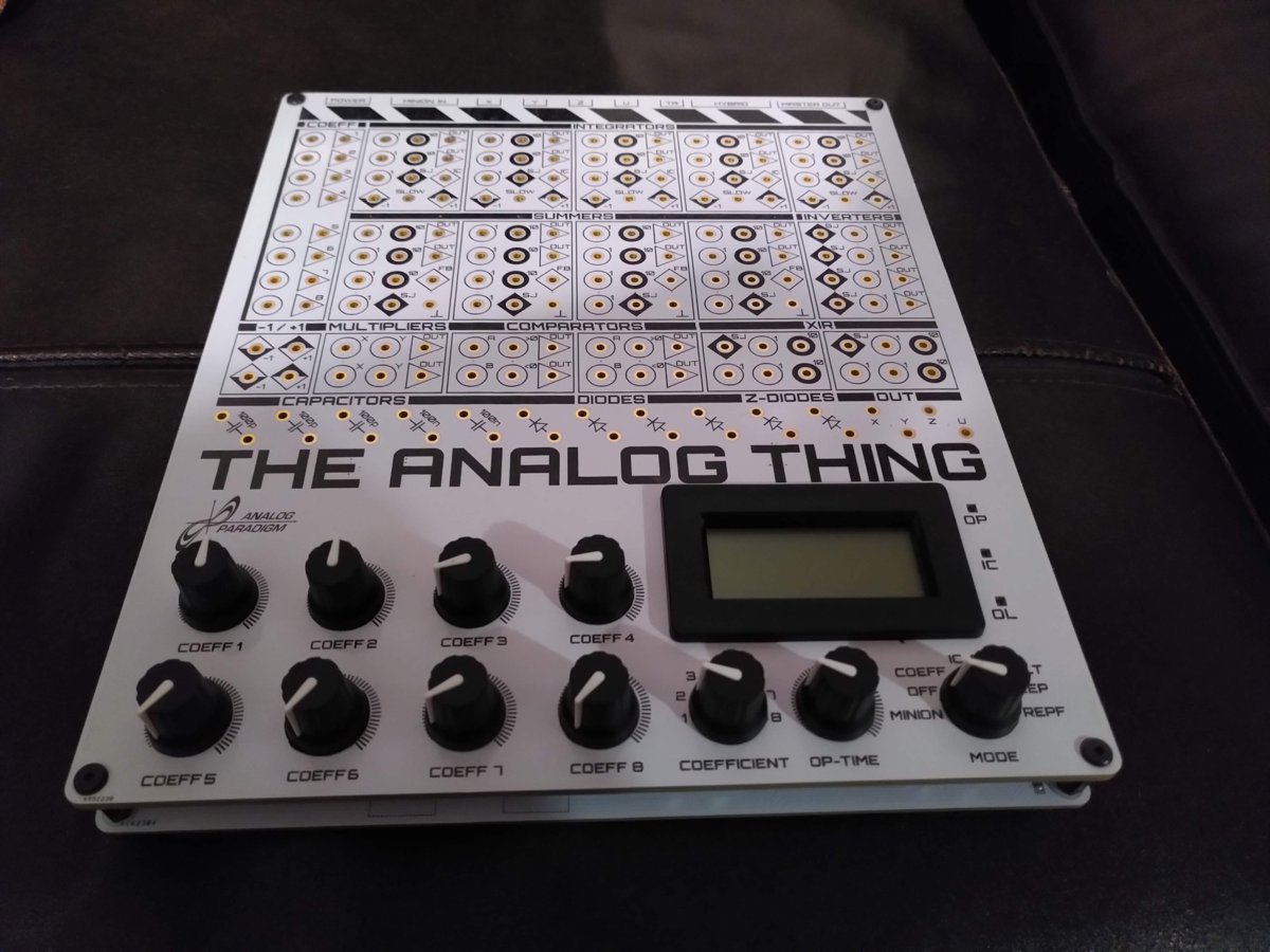
8.1 Panel / Jack Color Map
The THAT patch panel uses jack color and symbol to convey both signal role and weighting at a glance. The table below is the authoritative field reference; all values verified against the First Steps v2 manual (§8) and the V1.3 front-panel schematics.
Table 1 — Panel / Jack Color Map
| Jack color / marking | Symbol on panel | Signal role | Weight / notes |
|---|---|---|---|
| White circle — “1” | ○ 1 | Unweighted input | ×1 — signal passes unchanged |
| Black circle — “10” | ● 10 | Weighted input | ×10 — input is multiplied by 10 internally |
| Triangle | ▷ | Output | Computing-element output; stackable for fan-out |
| White diamond (top half black) — “+1” | ◈⁺ | Machine-unit source | Provides +1 MU (+10 V) |
| Black diamond (bottom half black) — “−1” | ◈⁻ | Machine-unit source | Provides −1 MU (−10 V) |
| White diamond — “IC” | ◇ IC | Initial condition input | Sets integrator output at start of run (inverted — see §3) |
| White diamond — “FB” | ◇ FB | Feedback jack (summers) | Bridging FB to GND opens the feedback resistor → open amplifier |
| Ground symbol — ”⏚“ | ⏚ | Chassis / signal ground | Reference; also used to disable FB |
| White diamond — “SLOW” | ◇ SLOW | Integrator speed reduction | Connecting INT output → SLOW reduces speed to 1/100 |
| SJ (unlabeled square) | □ SJ | Summing junction | Connect XIR SJ to element SJ to add inputs |
Note — Input jacks accept one cable only. Output jacks may be stacked (multiple plugs in one jack) to distribute a signal to several destinations. Never connect two outputs together; the resulting short will drive both op-amps into overload.
Tip — The ×10 weighted inputs (black circle, “10”) are most useful when a signal has been scaled far below full-scale and needs boosting without an extra summer. Patching a 0.05 MU signal into a ×10 input delivers 0.5 MU at the summing junction — equivalent to a ×10 gain stage with no additional element.
8.2 Element Quick-Reference
8.2.1 Inventory (verified from First Steps §7 and V1.3 front-panel schematics)
Table 2 — Inventory (verified from First Steps §7 and V1.3 front-panel schematics)
| Element | Count | Schematic labels | Input jacks | Output jacks | Special jacks |
|---|---|---|---|---|---|
| Integrator | 5 | INT1 – INT5 | 5 × (3 × ×1 white, 2 × ×10 black) + IC | 2 (INT-Out A/B) | SLOW |
| Summer | 4 | SUM1 – SUM4 | 7 × (4 × ×1 white, 3 × ×10 black) | 2 (SUM-Out A/B) | FB, ⏚ |
| Inverter | 4 | INV1/2, INV3/4 (2 per block) | 1 × ×1 | 2 (INV-Out A/B) | SJ |
| Multiplier | 2 | MUL1/2 | 2 (×-input, y-input) | 2 (MUL-Out) | — |
| Comparator | 2 | CMP1/2 | 3 (A, B, >, <) | 2 (CMP-Out) | — |
| Coeff. pot | 8 | PT1 – PT8 (COEFF1-8 block) | 1 (coeff input) | 1 (coeff output) | Selector knob |
| Resistor network | 2 | XIR1/2 | 4 (XIR inputs) | — | SJ |
| Machine unit src | 2 pairs | MU block (near INT group) | — | +1 jack, −1 jack | — |
| Diodes / Zeners | Several | D-block (panel) | Application-specific | Application-specific | — |
| Capacitors (panel) | Several | C-block (panel) | Application-specific | Application-specific | — |
Note — The total plug-board position count is 186 (confirmed First Steps FAQ). Integrators and summers invert sign implicitly — the output of a summer wired as Σ(a,b) delivers −(a+b).
8.2.2 Element Block Diagrams (ASCII)
INTEGRATOR (×1 of 5)                    SUMMER (×1 of 4)
┌─────────────────────────┐             ┌──────────────────────────┐
│  ○1  ─────┐             │             │  ○1  ──────┐             │
│  ○1  ─────┤             │             │  ○1  ──────┤             │
│  ○1  ─────┤  ∫dt  ▷▷── OUT           │  ○1  ──────┤  Σ   ▷▷── OUT
│  ●10 ─────┤  (−sign)    │             │  ○1  ──────┤  (−sign)    │
│  ●10 ─────┘             │             │  ●10 ──────┤             │
│  ◇IC                    │             │  ●10 ──────┤             │
│  ◇SLOW                  │             │  ●10 ──────┘             │
│  □SJ                    │             │  ◇FB  ◈⏚                 │
└─────────────────────────┘             └──────────────────────────┘

INVERTER (×1 of 4)                      MULTIPLIER (×1 of 2)
┌──────────────────┐                    ┌────────────────────────┐
│  ○1  ────  −1 ▷▷─ OUT                │  ○x ────┐              │
│  □SJ             │                    │  ○y ────┤  x·y  ▷▷── OUT
└──────────────────┘                    └────────────────────────┘

COMPARATOR (×1 of 2)                    COEFF POT (×1 of 8)
┌─────────────────────────┐             ┌────────────────────────┐
│  ○A ──┐                 │             │  ○IN ── [POT] ── ▷OUT  │
│  ○B ──┤ A+B>0 → ">" OUT │             │  Range: 0 to +1 MU     │
│  ○>  ─┤ A+B≤0 → "<" OUT │             │  Read via panel meter  │
│  ○<  ─┘          ▷▷──  │             │  in COEFF mode         │
└─────────────────────────┘             └────────────────────────┘
Note — Multiplier output is x · y with no sign inversion. Comparator routes whichever input (”> ” or ”<”) is active to its output; the routing, not arithmetic, is the function. Coefficient pots produce a value in [0, +1] from their output jack; to obtain a negative coefficient, run the pot output through an inverter, or feed −1 MU into the pot input and use the (now negated) pot output directly.
8.3 Scaling Formula Card (+/−10 V Machine Units)
8.3.1 Core Conventions
Table 3 — Core Conventions
| Symbol | Meaning |
|---|---|
| MU | Machine unit — the normalized ±1 interval; physical realization is ±10 V |
| x̂ | Problem variable (physical units, e.g., metres, amperes) |
| X | Machine variable; X = x̂ / x̂_max so |
| k_x | Scale factor for variable x: k_x = 1 / x̂_max |
| τ | Problem time constant (seconds) |
| τ_m | Machine time constant; τ_m = τ / β (β = time-scale factor) |
| β | Time-scale compression factor (β > 1 = faster, β < 1 = slower) |
8.3.2 Magnitude Scaling — Step-by-Step
1. Write the ODE in physical variables.
2. Identify the peak expected value of each variable: x̂_max.
3. Substitute X = x̂ · k_x  (k_x = 1/x̂_max) to normalize all
   variables to the ±1 MU range.
4. Rewrite the ODE in machine variables X. Collect scale factors
   on coefficient pots or ×10 inputs.
5. Check: no term exceeds ±1 MU at any expected operating point.
   Add a safety margin of ≥20% (keep peak at ≤0.8 MU).
8.3.3 Time Scaling — Key Relations
Machine time:  t_m = β · t_phys

Derivative transform:   dx̂/dt  →  (k_x / β) · dX/dt_m

Integrator equation:    X_out = −∫ Σ(weighted inputs) dt_m
                               = −∫ Σ(a_i · X_i) dt_m

Time constant at machine speed (β=1000, slow patch → SLOW jack):
  τ_m = τ_phys / β    e.g., τ_phys=1 s, β=1000 → τ_m=1 ms
8.3.4 Coefficient Pot Recipes
Table 4 — Coefficient Pot Recipes
| Goal | Patch action | Range |
|---|---|---|
| Coefficient c ∈ [0, +1] | +1 MU → POT input; read output | 0 to 1 |
| Coefficient c ∈ [−1, 0] | −1 MU → POT input; read output | −1 to 0 |
| Coefficient c ∈ [−1, +1] | +1 MU and −1 MU → summer → POT (see Vol 4 §4) | ±1 |
| Coefficient c > 1 | Use ×10 weighted input; POT provides c/10 | Up to 10 |
8.3.5 Overload Prevention Rules
┌────────────────────────────────────────────────────────────────┐
│  RULE 1  — Peak signal ≤ 0.8 MU on every node.                │
│  RULE 2  — Sum of inputs to any element ≤ 1.0 MU.             │
│  RULE 3  — If OL LED lights, halt (HALT mode), rescale,       │
│            then restart from IC.                               │
│  RULE 4  — High-frequency solutions: check for integrator      │
│            runaway in the first 10 ms (OP mode).              │
│  RULE 5  — In SLOW mode (SLOW jack connected), speed = 1/100. │
│            A 1 ms integration at normal speed takes 100 ms.   │
└────────────────────────────────────────────────────────────────┘
8.3.6 First-Order ODE Example (Radioactive Decay)
Physical:     ẋ = −λx,   x(0) = x₀
Machine:      Ẋ = −λX,   X(0) = X₀ = 1 (set IC pot to 1)

Patch:   +1 MU → [POT: λ] → INT1 (×1 input)
         INT1 output (−X) → back to INT1 (×1 input, gives +λX)
         Wait — integrator inverts → output is +X; feed −X
         back to get the correct sign: use INT1 output directly
         (the integrator already provides sign inversion).

        [IC=+1] ──◇IC──┐
                       INT1 ──▷──○ (=−X) ── back to INT1 ×1 input
                        ↑
                      [POT_λ] ← +1MU
Note — A single integrator whose output feeds its own input through a coefficient pot is the canonical first-order decay circuit. Adding a second integrator in the feedback loop solves second-order ODEs (see Vol 3 and Vol 4 for full derivations).
8.4 Patch Quick-Reference
8.4.1 Standard Patch Topologies
┌──────────────────────────────────────────────────────────────────┐
│  TOPOLOGY 1 — First-Order (1 integrator, direct feedback)        │
│                                                                  │
│   ẋ = −ax + u                                                   │
│                                                                  │
│   [u] ──○1── INT1 ──▷──○ (=−x)                                 │
│   [−x] ─────[POT a]──○1──┘  (re-enters INT1 as +ax)            │
│   IC: set to desired x(0) via IC jack (inverted: IC= −x₀)       │
└──────────────────────────────────────────────────────────────────┘

┌──────────────────────────────────────────────────────────────────┐
│  TOPOLOGY 2 — Second-Order (2 integrators, cascade)              │
│                                                                  │
│   ẍ = −ω²x − 2ζω ẋ + f(t)                                     │
│                                                                  │
│   [f(t)]─○1──┬─ INT1 ──▷─ (=−ẋ) ─○1─ INT2 ──▷─ (=x)          │
│   [x]──[ω²]──┘                                                  │
│   [ẋ]─[2ζω]──┘   (both re-enter INT1)                           │
│   IC1= +ẋ₀ (inverted),  IC2= −x₀ (inverted)                    │
└──────────────────────────────────────────────────────────────────┘

┌──────────────────────────────────────────────────────────────────┐
│  TOPOLOGY 3 — Multiplier (nonlinear term x·y)                    │
│                                                                  │
│   ẋ = −xy  (predator-prey cross term)                            │
│                                                                  │
│   [x] ──○x──┐                                                   │
│   [y] ──○y──┤ MUL1 ──▷── (=xy)                                 │
│              └── negate via INV, then feed to INT as input       │
└──────────────────────────────────────────────────────────────────┘

┌──────────────────────────────────────────────────────────────────┐
│  TOPOLOGY 4 — Comparator (conditional switching)                 │
│                                                                  │
│   if (A+B > 0): route signal_A to output                         │
│   else:         route signal_B to output                         │
│                                                                  │
│   [A] ──○A──┐                                                   │
│   [B] ──○B──┤ CMP1                                              │
│   [sig_A]──○>──┤    ──▷── (routed output)                       │
│   [sig_B]──○<──┘                                                │
└──────────────────────────────────────────────────────────────────┘
8.4.2 Helper-Function Patches (verified from First Steps §10)
Table 5 — Helper-Function Patches (verified from First Steps §10)
| Function | Elements needed | Key patch | Output range |
|---|---|---|---|
| max(A, B) | 1 CMP, 1 SUM | CMP: if A > 0→A, else→B; A+B sum drives decision | ±1 MU |
| min(A, B) | 1 CMP, 1 SUM | Inverse comparator routing | ±1 MU |
| abs(A) | 1 CMP, 1 INV | CMP routes A or INV(A) based on sign of A | 0 to +1 |
| clamp(A, 0) | 1 CMP | Route A when A>0, route 0 (GND) otherwise | 0 to +1 |
| c ∈ [−1,+1] | 1 POT, 1 SUM, 2 MU | +1 MU and −1 MU summed with pot in loop | −1 to +1 |
| Division A/B | 1 MUL + open SUM | Open-amp feedback through multiplier | ±1 MU |
| √A | 1 MUL + open SUM | MUL in feedback around open-amp summer | 0 to +1 |
Tip — To implement division A/B, disable the summer’s feedback resistor (FB jack → GND), connect the output back through a multiplier, and feed the product back as the negative feedback signal. The equilibrium forces output × B = A, so output = A/B. See Vol 3 §7 for the full derivation.
8.4.3 Signal-Flow Conventions
  ─── solid line: patch cable connection
  ○   circle at junction: input jack (single cable only)
  ▷   triangle: output jack (stackable)
  [ ] bracket: labeled sub-element (e.g., [POT a], [MUL1])
  ◇   diamond: special-purpose jack (IC, SLOW, FB)
  ⏚   ground reference
  →   signal direction
8.5 Mode + Time-Constant Switch Reference
8.5.1 Operating Modes (Mode Selector)
Table 6 — Operating Modes (Mode Selector)
| Mode | Panel LED | Integration | Coefficient display | Typical use |
|---|---|---|---|---|
| COEFF | — | Frozen | Pot selected by COEFF knob shown on panel meter (0 to 1) | Set pot values before run |
| IC | IC (green) | Frozen — outputs driven to IC values | — | Load initial conditions into integrators |
| OP | OP (green) | Running | U-output value on panel meter (±1) | Single continuous run |
| HALT | — | Frozen — outputs held at last values | — | Pause and inspect mid-run |
| REP | OP (cycling) | IC → OP → IC → … (period set by OP-TIME pot, 0–10 s) | OP-TIME shown on meter | Oscilloscope steady-state display; slow problems |
| REPF | OP (cycling fast) | IC → OP → IC → … (period 0–100 ms, ×100 faster) | OP-TIME shown 0–100 ms | Fast display on scope; use with TRIG output |
| MINION | — | Controlled by MASTER unit | — | Multi-unit chained operation |
Note — The OP-Time potentiometer on the front panel sets the time spent in OP mode per REP/REPF cycle. The IC phase is brief and automatic. The RCA TRIG output fires at the start of each IC phase, providing a reliable oscilloscope trigger for REP and REPF.
8.5.2 Time-Constant Control: The SLOW Jack
┌────────────────────────────────────────────────────────────────┐
│  SLOW jack — per integrator, independent                        │
│                                                                  │
│  Not connected (normal speed):                                  │
│    −1 MU input, IC = 0 → output reaches +1 MU in 1 ms         │
│    Time constant τ_m = 1 ms per unit input                      │
│                                                                  │
│  SLOW jack connected (INT output looped to INT SLOW jack):      │
│    −1 MU input, IC = 0 → output reaches +1 MU in 100 ms        │
│    Time constant τ_m = 100 ms per unit input (1/100 speed)      │
│                                                                  │
│  Combined with REPF (100 ms window): SLOW integrators useful    │
│  for very low-frequency dynamics within the 100 ms OP window.   │
└────────────────────────────────────────────────────────────────┘
8.5.3 Mode Sequence Checklist
  Before first run:
  ① COEFF mode → set all pots (verify on panel meter)
  ② IC mode → confirm IC LED, check initial-condition nodes on scope
  ③ OP mode → single run; watch for OL LED
  ④ HALT mode (if needed) → inspect held values
  ⑤ REP or REPF → for scope display; adjust OP-TIME pot

  If OL (overload) LED lights:
  → Switch to HALT immediately
  → Identify which element overloaded (check all nodes)
  → Rescale the offending variable (reduce pot gain or rebalance)
  → Return to IC mode and re-run
8.6 Daisy-Chain / HYBRID Wiring Card
8.6.1 MASTER / MINION Chain
  MASTER THAT                 MINION THAT #1              MINION THAT #2
  ┌──────────────┐            ┌──────────────┐            ┌──────────────┐
  │              │  ribbon    │              │  ribbon    │              │
  │  MASTER OUT ─┼────────────┼→ MINION IN   │            │              │
  │  (rear port) │  cable     │  MASTER OUT ─┼────────────┼→ MINION IN   │
  │              │            │  (rear)      │  cable     │              │
  │  Mode: sets  │            │  Mode:       │            │  Mode:       │
  │  all modes   │            │  MINION      │            │  MINION      │
  └──────────────┘            └──────────────┘            └──────────────┘

  Shared via ribbon: IC/OP/HALT/REP/REPF control signals
  Chain length: unlimited (no documented limit in First Steps)
  Cable: included ribbon cable (MASTER OUT → MINION IN)
Note — Each MINION is set to MINION mode on its own Mode Selector. All timing (IC/OP/HALT/REP/REPF) is controlled exclusively from the MASTER unit. The MASTER’s front-panel OP-TIME pot sets the cycle time for the entire chain.
8.6.2 Inter-Unit Signal Patching
  ┌─────────────────────────────────────────────────────────────┐
  │  Signal sharing between units uses patch cables directly:   │
  │                                                             │
  │  MASTER output jack ──[patch cable]──→ MINION input jack    │
  │  MINION output jack ──[patch cable]──→ MASTER input jack    │
  │                                                             │
  │  Signals are standard ±10 V patch-level — no attenuation   │
  │  needed for unit-to-unit patch connections.                 │
  │                                                             │
  │  Output jacks X, Y, Z, U (rear RCA) carry the signals      │
  │  patched to the matching front-panel output jacks,          │
  │  attenuated to ±1 V for audio interface / scope use.        │
  └─────────────────────────────────────────────────────────────┘
8.6.3 HYBRID Port (Digital Interface)
Table 7 — HYBRID Port (Digital Interface)
| Signal direction | Connector | Voltage range | Notes |
|---|---|---|---|
| Analog → Digital | HYBRID port (rear) | 0 to 3.3 V (shifted & attenuated from ±10 V) | ADC-compatible; use for data logging |
| Digital → Analog | HYBRID port (rear) | 0 to 3.3 V | Controls OP/IC/HALT mode from microcontroller or FPGA |
| Rear RCA X/Y/Z/U | RCA jacks (rear) | ±1 V | Attenuated from patch jacks X/Y/Z/U; scope / audio-interface compatible |
| RCA TRIG Out | RCA jack (rear) | Pulse | Fires at IC→OP transition in REP/REPF; use for scope trigger |
Tip — To log a run to a PC without an oscilloscope, connect the rear RCA X and Y outputs to a stereo USB audio interface, run any oscilloscope or data-acquisition software (e.g., Audacity, MATLAB, Python sounddevice), and set THAT to REP mode. The audio interface’s DC-blocking capacitors will distort low-frequency components — adequate for qualitative work, not for quantitative scaling. See Vol 6 for workarounds using DC-coupled DAQ hardware.
8.6.4 Multi-Unit Element Budget
Table 8 — Multi-Unit Element Budget
| Units in chain | Total integrators | Total summers | Total multipliers | Total comparators | Total coeff pots |
|---|---|---|---|---|---|
| 1 | 5 | 4 | 2 | 2 | 8 |
| 2 | 10 | 8 | 4 | 4 | 16 |
| 3 | 15 | 12 | 6 | 6 | 24 |
| N | 5N | 4N | 2N | 2N | 8N |
8.7 Quick-Start Checklist
8.7.1 Hardware Setup
  □ 1. Connect USB-C power (5 V / ≥500 mA USB supply; USB data not used)
  □ 2. Connect scope / display:
         Option A: BNC → rear RCA X/Y/Z/U via RCA-BNC adapter (±1 V, AC-coupled)
         Option B: USB audio interface → rear RCA (stereo, ±1 V)
         Option C: direct patch cable from output jacks to DVM for DC spot checks
  □ 3. For REP/REPF: connect TRIG out (rear RCA) to scope external trigger
  □ 4. If multi-unit: connect MASTER OUT → MINION IN ribbon cable;
         set MINION(s) to MINION mode
  □ 5. Confirm power: State LEDs should be dark (no mode active yet)
8.7.2 Programming Sequence
  □ 6.  Write the governing ODE(s)
  □ 7.  Apply magnitude scaling: X = x̂ / x̂_max for each variable
  □ 8.  Apply time scaling: choose β so that OP-TIME window captures the dynamics
  □ 9.  Draw the patch diagram (use template at the-analog-thing.org/THAT_template.pdf)
  □ 10. Identify coefficient values; note which pots are needed
  □ 11. Set Mode Selector → COEFF
  □ 12. Use COEFF SELECTOR knob to select each pot; adjust knob;
          confirm value on panel meter (0 to 1 scale)
  □ 13. Set Mode Selector → IC
  □ 14. Apply patch cables per diagram (output → input only; never output → output)
  □ 15. Check IC values at integrator outputs on scope
8.7.3 Running and Debugging
  □ 16. Set Mode Selector → OP (single run) or REP / REPF (repetitive)
  □ 17. Watch OL LED — if it lights, immediately → HALT
  □ 18. Adjust scope: 2-channel X/Y or time-domain; set vertical sensitivity
          to ≈2 V/div for ±10 V signals (direct patch-level) or 200 mV/div (RCA)
  □ 19. Verify qualitative behavior vs. expected phase portrait or time trace
  □ 20. Fine-tune coefficients: return to COEFF mode, adjust, re-run
  □ 21. Quantitative measurement: HALT at a point of interest;
          read U output on panel meter; or capture with scope/DAQ
Note — If fingerprints or contamination on the patch panel cause integrators to drift into overload with no patch connected, clean the panel gently with isopropyl alcohol on a lint-free cloth. This is confirmed as a resolution in the First Steps FAQ.
Tip — For chaotic systems (Lorenz, Duffing), place the scope in X-Y mode using two integrator outputs. The attractor geometry is immediately visible without triggering. See Vol 5 for annotated Lorenz and Van der Pol patches.
8.8 Specification Card
8.8.1 Electrical Specifications
Table 9 — Electrical Specifications
| Parameter | Value | Source |
|---|---|---|
| Machine unit range | ±1 (conceptual) / ±10 V (physical) | First Steps §5 |
| Internal supply voltage | ±12 V (generated on-board) | First Steps FAQ |
| Input power | 5 V DC via USB-C | First Steps §1 |
| Input power source | USB-C (data pins unused); USB power supply or hub | First Steps §1 |
| Maximum external voltage | ±12 V (hard limit; >±12 V risks damage) | First Steps warning |
| RCA output level | ±1 V (attenuated from ±10 V) | First Steps §3 |
| HYBRID port output level | 0 to 3.3 V (shifted from ±10 V) | First Steps §5 |
| Precision | ~2 decimal digits relative to MU | First Steps FAQ |
| Normal integrator speed | Full-scale (0 → ±1) in 1 ms | First Steps §8 |
| SLOW integrator speed | Full-scale in 100 ms (1/100 normal) | First Steps §8 |
| REP OP-TIME range | 0 to 10 seconds | First Steps §14 |
| REPF OP-TIME range | 0 to 100 ms | First Steps §14 |
| Recommended scope bandwidth | ≥200 kHz (ideal); ≥20 kHz (minimum usable) | First Steps §6 |
| Patch field positions | 186 total plug positions | First Steps FAQ |
| Plug type | 2 mm banana plug | First Steps §3 |
8.8.2 Computing-Element Summary
Table 10 — Computing-Element Summary
| Element | Count | Key characteristics |
|---|---|---|
| Integrators | 5 | 5 inputs (2 × ×10); IC jack; SLOW jack; 2 outputs; sign-inverting |
| Summers | 4 | 7 inputs (3 × ×10); FB jack for open-amp mode; 2 outputs; sign-inverting |
| Inverters | 4 | 1 input; 2 outputs; SJ jack for extension |
| Multipliers | 2 | 2 inputs (x, y); 2 outputs; no sign inversion |
| Comparators | 2 | A, B threshold inputs; >, < signal inputs; 2 outputs; routes, does not compute |
| Coefficient pots | 8 | Range 0 to 1 (single direction); panel-meter readout in COEFF mode |
| Resistor networks | 2 | SJ-to-SJ connection extends summers/integrators/inverters |
8.8.3 Physical & Interface
Table 11 — Physical & Interface
| Parameter | Value |
|---|---|
| Form factor | Desktop / benchtop module |
| Power connector | USB-C (rear) |
| Display output | 4 × RCA jacks (X, Y, Z, U) — rear; ±1 V |
| Trigger output | 1 × RCA (TRIG) — rear |
| HYBRID port | 1 × multi-pin connector — rear (0 to 3.3 V) |
| MASTER OUT / MINION IN | 2 × ribbon connectors — rear |
| Panel meter | 3.5-digit display; COEFF (0–1) or signal (±1) or OP-TIME |
| State LEDs | OP (green), IC (green), OL (red — overload) |
| Patch cable set (included) | 30 × 2 mm banana plug cables |
| Included cables | 1 × USB-A to USB-C power; 1 × stereo RCA-RCA; 1 × ribbon (MASTER-MINION) |
| Open hardware | Yes — schematics CC-licensed; GitHub: github.com/anabrid/the-analog-thing |
| Software | None required for standalone operation |
| Manufacturer | anabrid GmbH, Berlin, Germany |
| Contact / shop | [email protected] / shop.anabrid.com |
8.8.4 Volume Cross-Reference Index
Table 12 — Volume Cross-Reference Index
| Topic | Primary volume | Secondary |
|---|---|---|
| THAT history, Anabrid, open-hardware ethos | Vol 1 | — |
| Full schematic walk (Base 01–05, Front 01–02) | Vol 2 | — |
| Computing elements in depth (integrators, summers…) | Vol 3 | Vol 2 |
| Magnitude scaling, time scaling, coefficient setting | Vol 4 | Vol 3 |
| Worked examples: Lorenz, pendulum, predator-prey… | Vol 5 | Vol 4 |
| HYBRID port, daisy-chain, digital interfacing | Vol 6 | — |
| THAT vs EC-1, big iron, modern kits; buying guide | Vol 7 | Vol 1 |
| This cheatsheet | Vol 8 | All |
Note — All element counts in this volume are verified from two independent sources: the First Steps v2 manual (Anabrid, 2023) and the V1.3 front-panel schematics (analog_thing_front V1.3, 03.2022, Analog Paradigm). Any parameter not confirmed by those sources is explicitly flagged as unverified.
Comments (0)