THAT — The Analog Thing · Volume 4
THE Analog Thing — Volume 4 — Programming
Turning differential equations into patches: scaling, timing, and coefficient setting on THAT
4.1 About This Volume
Volumes 1 through 3 of this series establish hardware architecture, the computing elements, and the electrical specification of THE Analog Thing (THAT). Volume 4 is the programmer’s manual: it explains how to translate a mathematical description of a dynamic system into a working patch on THAT’s front panel, how to keep all signals within the ±10 V machine unit, and how to observe and interpret results. Volume 5 covers multi-unit Master/Minion chains; Volume 6 covers hybrid digital/analog interfacing via the HYBRID port.
Scope — All element counts, voltage levels, and mode labels in this volume are verified against the THAT v1.3 schematics (Analog Paradigm, 2022) and the First Steps guide v2.0 (Fischer & Ulmann, 2023). No values have been inferred or extrapolated from outside sources.
4.1.1 The machine unit and its physical voltage
THAT represents every problem quantity as a voltage in the closed interval −10 V to +10 V. The programmer never works directly with volts; instead, the machine unit (MU) is defined as ±1, where +1 corresponds to +10 V and −1 corresponds to −10 V. The translation is exact and linear:
$$V = 10 \times u, \qquad u \in [-1,;+1]$$
A DC/DC converter on the Base PCB steps the 5 V USB-C supply up to a regulated ±12 V rail; the ±10 V machine unit is derived from that rail, leaving a 2 V headroom before the op-amps saturate and the OL (overload) LED illuminates. The overload comparator trips at approximately ±10 V; any signal that exceeds ±1 MU clips and the corresponding output is unusable.
4.1.2 Element inventory
The table below is the authoritative resource count for a single THAT v1.3 unit, read from the Front PCB schematic (THAT-Front_v1.3_01/02.png).
Table 1 — Element inventory
| Computing element | Count | Designation on schematic |
|---|---|---|
| Integrators | 5 | INT1 … INT5 |
| Summers | 4 | SUM1 … SUM4 |
| Inverters | 4 | INV1/2, INV3/4 (two per block) |
| Multipliers | 2 | MUL1, MUL2 |
| Comparators | 2 | CMP1, CMP2 |
| Coefficient potentiometers | 8 | COEFF1 … COEFF8 |
| Resistor networks (XIR) | 2 | XIR1, XIR2 |
| Machine unit jacks (+1 / −1) | multiple | grouped with integrators |
| Diodes / Zener diodes | provided | discrete, on Base PCB |
| Capacitors (patch-accessible) | provided | discrete, on Base PCB |
Table 1 — Computing element inventory, THAT v1.3 (single unit)
Each integrator provides five input jacks: three weighted ×1 (white circles) and two weighted ×10 (black circles), plus an IC (initial condition) jack and a SLOW jack. Each summer provides seven input jacks: four weighted ×1 and three weighted ×10. Each integrator and each summer exposes a Summing Junction (SJ) jack so that a resistor network (XIR) can augment the input count. Inverters expose one input jack and two output jacks (stacked for fanout). Multipliers expose two input jacks and two output jacks.
4.2 The Method — Turning an ODE into a Patch
Analog computer programming rests on a single insight: a chain of integrators driven by a feedback signal continuously satisfies the differential equation it was derived from. The standard workflow is known as the Kelvin feedback technique.
4.2.1 Step 1 — Write the equation in standard form
Isolate the highest derivative on the left-hand side. For an nth-order ODE the left side reads x⁽ⁿ⁾ and the right side is a function of lower derivatives and independent variables:
x'' = f(x', x, t)For a second-order equation this gives x” on the left. If x” is assumed to be available as a voltage at an output jack, everything on the right-hand side can be formed by combining that signal with weighted copies of itself integrated once and twice.
4.2.2 Step 2 — Draw the integrator chain
Each integration step:
- produces the next lower derivative at its output jack, and
- inverts sign (integrators on THAT are inverting; this is the standard op-amp topology).
For x” → x’ → x the patch uses two integrators in series:
                 ┌──────────────────────────────────────┐
                 │             feedback                  │
                 ▼                                       │
  (assumed x'')──[INT1]──(−x')──[INT2]──(x)─────────────┤
                   │                     │              │
                  −x'                    x          (to adder)
Because INT1 inverts, its output is −x’. Because INT2 inverts −x’, its output is +x. The sign tracking must be done explicitly at every node.
4.2.3 Step 3 — Form the right-hand side
The right-hand side of the ODE is assembled from summers, inverters, multipliers, and coefficient potentiometers fed by taps from the integrator chain. The output of this network must equal the assumed x” — this closes the feedback loop. If the signs do not match, add an inverter.
4.2.4 Step 4 — Set initial conditions
Each integrator holds an initial-condition voltage on its IC jack. In IC mode (mode selector to IC), the integrator output is driven to −IC_input (inverted). Setting IC = −x₀ therefore yields output = +x₀ at t=0 when OP begins. IC jacks accept any signal in the ±1 MU range, including outputs of coefficient potentiometers set to the desired starting value.
4.2.5 Step 5 — Verify sign conventions at every node
A sign error is the most common patching mistake. The recommended practice is to annotate each wire in the patch diagram with its sign relative to the highest derivative. THAT provides both output jacks of integrators and summers; the second jack is a duplicate for fanout — both carry the same polarity.
4.2.6 Signal-flow example: first-order decay
The simplest closed patch: one integrator, one coefficient potentiometer.
   ┌─────────────────────────────────────────┐
   │                  λ                       │
   │   +1 ──[POT1]──× ──────────────────────►│
   │                                          │
   │          ┌──────────────────────────┐    │
   └──────────► INT1  (SLOW connected)   ├────┘
              │  IC: −N₀                 │
              └──────────┬───────────────┘
                         │ output = +N(t)
                         ▼
                     [INV1] ──► display
The differential equation modelled is dN/dt = −λN. The integrator inverts, so feeding its output back to its own input (via a potentiometer for λ) implements negative-feedback decay. An inverter after the integrator recovers the positive display variable N(t).
4.3 Magnitude Scaling on a ±10 V Machine
4.3.1 Why overload matters
When any node voltage exceeds ±10 V the associated op-amp saturates. The OL LED illuminates and the offending integrator or summer locks its output at the rail. Because integrators in feedback loops drive each other, a single overload cascades through the patch within microseconds, destroying all computed signals. The machine unit headroom — 2 V above ±10 V before the ±12 V rail — is not usable signal range; it is a safety margin only.
Rule — Design so that the maximum excursion of every node stays below |0.9 MU| in normal operation. Leaving 10 % headroom accommodates parameter excursions during interactive tuning.
4.3.2 Magnitude scaling procedure
Let the raw problem variable be Q with physical peak value Q_max. Define the scaled machine variable:
$$u_Q = \frac{Q}{Q_{\max}}$$
so that |u_Q| ≤ 1. Every coefficient involving Q must be adjusted by the same factor so that the equations remain consistent.
Scaling table — mass-spring-damper example
The raw equation is my” + Dy’ + sy = 0, resolved as:
$$y” = \frac{1}{m}\left(-Dy’ - sy\right)$$
Estimated physical peaks: y_max = A (displacement), y’_max = ωA (velocity), y”_max = ω²A (acceleration). Define u_y = y/A, u_v = y’/(ωA), u_a = y”/(ω²A).
Table 2 — Magnitude scaling procedure
| Node | Raw variable | Scale factor | Machine variable |
|---|---|---|---|
| Acceleration | y” | 1/(ω²A) | u_a |
| Velocity | y’ | 1/(ωA) | u_v |
| Displacement | y | 1/A | u_y |
After substitution, the coefficients in the scaled equation become D/(mω) and s/(mω²). Both must fall in (0,1] for the coefficient potentiometers to implement them directly. If a computed coefficient exceeds 1, use the ×10 weighted inputs (black circles) to provide an implicit factor of ten, reducing the required pot setting by ×0.1.
4.3.3 Using the ×10 weighted inputs for implicit gain
Every integrator and summer input marked with a black circle multiplies the incoming signal by 10 before presenting it to the summing junction. This is not a separate element; it is a built-in resistor ratio. Connecting a signal carrying value u to a ×10 input and setting the coefficient potentiometer to α delivers an effective gain of 10α — useful when the scaled coefficient is between 1 and 10 and re-scaling the problem variable is inconvenient.
Table 3 — Using the ×10 weighted inputs for implicit gain
| Input marking | Symbol | Effective gain with pot at α |
|---|---|---|
| White circle, “1” | ×1 | α (range 0 to 1) |
| Black circle, “10” | ×10 | 10α (range 0 to 10) |
Table 2 — Input weighting on integrators and summers
4.3.4 Scaling tree diagram
The diagram below illustrates how a second-order system with three nodes maps its peak excursions into the machine unit interval. Widths represent voltage headroom; each bar must fit within ±1 MU.
  MU ─────────────────────────────────────────────── +1.0
  0.9 ─────────────────────────────────────          ← design ceiling
          ██████████████████████████  u_a  peak ≈ 0.85
          ████████████████            u_v  peak ≈ 0.60
          ████████████████████████    u_y  peak ≈ 0.75
  0.0 ──────────────────────────────────────────────  0
         (mirrored below zero line by symmetry)
  −1.0 ─────────────────────────────────────────── −1.0
Figure 1 — Magnitude scaling target: all nodes inside ±0.9 MU
If any node peak exceeds 0.9 MU, divide that problem variable by a larger scale factor (or equivalently reduce the corresponding coefficient).
4.3.5 Overload indicators and diagnosis
THAT provides three State LEDs: OP (green — patch running), IC (yellow — initial condition phase), OL (red — overload active). When OL illuminates during a patch run:
- Switch to HALT mode immediately to freeze the outputs.
- Connect the panel meter to each node in turn (via the U output jack) to locate the offending signal.
- Reduce the scale factor of the overloading variable by 2× and re-derive affected coefficients.
Tip — The panel meter reads ±1 MU in IC, OP, and HALT modes when the U output jack is patched. In COEFF mode it reads the selected potentiometer value in the range 0 to 1.
4.4 Time Scaling and the Time-Constant Switches
4.4.1 The integrator time constant
An unmodified THAT integrator with a ×1 input connected to −1 MU and IC = 0 reaches +1 MU output in exactly 1 ms (from the First Steps manual, Section 8). This defines the base time constant τ = 1 ms per machine unit of input.
Equivalently: the integrator integrates at a rate of 1 MU/ms when driven by a 1 MU input signal. For a sinusoid at angular frequency ω (rad/ms) the integrator introduces a gain of 1/ω and a 90° phase lag — the standard op-amp integrator characteristic.
4.4.2 SLOW mode — reducing speed by 100×
Connecting an integrator’s output jack back to its own SLOW jack (a dedicated input jack on each integrator) introduces an additional RC time constant that extends the integration time to 100 ms per machine unit, a factor of 100 slowdown. This is implemented entirely by a passive resistor/capacitor network accessed through the SLOW jack; no mode switch is required.
Table 4 — SLOW mode — reducing speed by 100×
| Connection | Time constant | Rate |
|---|---|---|
| No SLOW connection | τ = 1 ms/MU | 1 MU per ms for 1 MU input |
| Output → SLOW jack | τ = 100 ms/MU | 1 MU per 100 ms for 1 MU input |
Table 3 — THAT integrator speed modes (verified from First Steps v2.0 §8)
Each integrator can independently have its SLOW jack connected or left open. Mixed-speed patches — some integrators fast, others slow — are legitimate and are used in the neuronal bursting example (Section 9.4 of First Steps), where the slow ion-channel integrator runs 100× more slowly than the two fast integrators.
4.4.3 The mode selector and repetitive operation
Time scaling at the patch level is complemented by the OP-Time potentiometer and the REP/REPF mode selector positions, which control how long each OP interval lasts between automatic IC resets.
Table 5 — The mode selector and repetitive operation
| Mode | OP interval range | Typical use |
|---|---|---|
| OP | Unlimited (manual HALT) | Single long run, interactive |
| HALT | — | Freeze outputs for measurement |
| IC | — | Set initial conditions (manual) |
| REP | 0 to 10 seconds | Slow patches, oscilloscope roll mode |
| REPF | 0 to 100 ms | Fast patches, oscilloscope X-Y mode |
| COEFF | — | Pot-setting mode (no patch running) |
| MINION | — | Slave to Master unit |
Table 4 — Mode selector positions and OP-time ranges
In REP and REPF modes, THAT automatically alternates between a brief IC phase (to reload initial conditions) and the OP phase (to run the patch). The Trigger Out RCA jack on the rear panel emits a synchronisation pulse at the start of each OP phase, enabling oscilloscope external triggering for flicker-free displays.
Tip — For phase-plane (X-Y) displays, REPF at 80 ms OP time typically yields a flicker-free Lissajous figure on most digital oscilloscopes. Increase OP time if the trajectory appears truncated before it closes.
4.4.4 Time scaling by coefficient selection
For phenomena whose natural time scale differs from THAT’s 1 ms base constant, the problem can be re-scaled in time by the factor k_t. If the natural period is T_natural and the desired patch period is T_patch:
$$k_t = \frac{T_{\text{patch}}}{T_{\text{natural}}}$$
Every velocity and rate coefficient in the scaled ODE is multiplied by k_t. For example, a chemical reaction with τ_natural = 1 s mapped to T_patch = 10 ms uses k_t = 0.01; all time-derivative coefficients shrink by 0.01, which is easily achievable with the coefficient potentiometers without needing the SLOW jacks. Conversely, a multi-decade orbital simulation compressed to 100 ms uses a large k_t and may require the ×10 inputs to implement the inflated coefficients.
   Time scaling relationship:

   T_natural   |  k_t   | Technique
   ────────────|────────|─────────────────────────────────────────
   ~1 ms       | 1.0    | Use integrators at normal speed
   ~100 ms     | 0.01   | Normal speed, reduce all coefficients ×0.01
   ~1 s        | 0.001  | Normal speed or SLOW mode on all integrators
   ~10 s       | 0.0001 | SLOW mode (×0.01) + coefficient reduction ×0.01
   ~1 ms fast  | 100    | REPF mode; scale coefficients ×100 with ×10 inputs
Table 5 — Time scaling strategies
4.5 Setting Coefficients
4.5.1 The eight coefficient potentiometers
COEFF1 through COEFF8 are single-turn potentiometers with a graduated (not numbered) dial, adjustable from 0 to 1. Each potentiometer has an input jack and an output jack on the patch panel. The procedure for setting a specific value:
- Connect the potentiometer’s input jack to the +1 machine unit jack.
- Switch THAT to COEFF mode.
- Rotate the Coefficient Selector knob to the desired potentiometer number (1–8).
- The Panel Meter displays the current output in the range 0 to 1.
- Adjust the potentiometer knob until the meter reads the target value.
- Return THAT to IC or OP mode when all potentiometers are set.
Note — The coefficient selector and panel meter display only one potentiometer at a time. Set all required potentiometers before leaving COEFF mode, then switch to IC to verify initial conditions.
The output of each potentiometer (connected as a voltage divider between the input signal and ground) feeds one or more computing element inputs. The potentiometer output jack is an output — do not connect multiple signal sources to it.
4.5.2 Negative coefficients
Coefficient potentiometers are unipolar: they output values in [0, +1] of their input. To implement a negative coefficient −α, connect the potentiometer input to the −1 machine unit jack instead of +1. The output is then −α, suitable for direct connection to a ×1 input jack of an integrator or summer.
Alternatively, connect the potentiometer output to a ×1 input of an inverter and use the inverter output; this preserves the flexibility to change sign by re-patching the potentiometer input between +1 and −1.
4.5.3 The adjustable ±1 helper circuit
Section 10.4 of First Steps documents a helper circuit (using a comparator) that extends the single potentiometer range from [0,1] to [−1,+1]. This is used in the polynomial generator example (Section 9.9) so that coefficients a, b, c, d can each be swept across the full machine unit range interactively.
4.5.4 Coefficient summary table
Table 6 — Coefficient summary table
| Potentiometer | Typical role | Range with +1 input | Range with −1 input |
|---|---|---|---|
| COEFFn (×1 input) | Coefficient 0 to 1 | 0 to +1 MU | 0 to −1 MU |
| COEFFn (×10 input) | Coefficient 0 to 10 | 0 to +10 MU | 0 to −10 MU |
| COEFFn (helper ±1 circuit) | Full bipolar sweep | −1 to +1 MU | +1 to −1 MU |
Table 6 — Coefficient potentiometer ranges by connection method
4.5.5 Stacking outputs for multiple destinations
A coefficient potentiometer output (like any output jack on THAT) can drive multiple destinations by physically stacking banana plugs into the same jack. There is no limit specified in the documentation, but practical stacking depth is 2–3 plugs before mechanical reliability decreases. For wider fanout, route through an inverter pair (to restore sign) or use the duplicate output jacks provided on each integrator and summer.
4.5.6 Resistor networks for extended input count
When an integrator or summer requires more inputs than its native jacks provide, a resistor network (XIR) can be connected via the SJ (summing junction) jacks. Both the computing element and the XIR expose an SJ jack; connecting these two SJ jacks together merges the resistor networks at the virtual ground of the op-amp input. Each XIR provides additional ×1 and ×10 input jacks. THAT includes two XIR units (XIR1, XIR2).
Note — The SJ jack is a true summing junction (virtual ground node), not an output. Do not connect an SJ jack to any output jack; doing so will force the virtual ground potential to a non-zero value, degrading accuracy across the entire element.
4.6 Reading Results — Display, Scope, and X-Y
4.6.1 The panel meter
THAT’s built-in panel meter (a 3½-digit LCD) serves two purposes depending on mode:
Table 7 — THAT's built-in panel meter (a 3½-digit LCD) serves two purposes depending on mode
| Mode | Meter reading | Range |
|---|---|---|
| COEFF | Selected potentiometer output | 0 to 1 |
| IC, OP, HALT, MINION | Value patched to U output jack | −1 to +1 |
| REP | OP-Time setting | 0 to 10 s |
| REPF | OP-Time setting | 0 to 100 ms |
Table 7 — Panel meter display modes
In OP mode, the meter provides a slow-update numerical read of whatever is patched to the U output jack on the front panel. This is ideal for monitoring DC or slowly-varying signals (population levels, fuel quantity in the lunar lander example) but it is too slow for signals varying faster than a few hertz.
4.6.2 The four output jacks (X, Y, Z, U)
The front panel carries four labelled output jacks: X, Y, Z, U. Patching any signal to one of these jacks routes that signal to both:
- the corresponding RCA Out jack on the rear panel, attenuated to ±1 V range (audio-compatible); and
- the HYBRID port on the rear panel, level-shifted to 0–3.3 V (for microcontroller ADC inputs).
The X, Y, Z, U jacks are inputs on the front panel (accepting a patch cable from any computed signal) and outputs on the rear panel. Do not confuse the two.
4.6.3 Oscilloscope connection
Connect the rear-panel RCA Out X (and Y for dual-channel) to the oscilloscope inputs using the included RCA-to-RCA cable and appropriate RCA-to-BNC adapters (not included). THAT’s output is ±1 V at the RCA jacks (10:1 attenuated from the ±10 V front-panel signals). Set oscilloscope input sensitivity to ≈ 200 mV/div for full-scale visibility.
THAT supports oscilloscope frequencies up to 200 kHz (from the First Steps requirements section). Software oscilloscopes via audio input interfaces work down to approximately 20 kHz — adequate for most patch problems but note that audio interfaces insert AC-coupling capacitors that remove DC components, distorting exponential and step signals.
4.6.4 Time-domain display (roll mode)
In REP mode with OP time set to 1–10 seconds, set the oscilloscope to roll mode (continuous sweep without trigger). The patch runs in real time; the user can adjust coefficients by rotating the potentiometer knobs and observe the waveform shift immediately.
4.6.5 Phase-plane (X-Y) display
The most informative display for two-dimensional autonomous systems (predator-prey, Lorenz, Euler spiral) is the X-Y mode, which plots one state variable against another rather than against time.
- Patch the first state variable to OUT X.
- Patch the second state variable to OUT Y.
- Set the oscilloscope to X-Y mode.
- Run THAT in REPF mode at an OP time that traces the trajectory in 30–100 ms for flicker-free rendering.
The Trigger Out RCA jack provides a rising-edge pulse at the start of each OP interval; connect this to the oscilloscope’s external trigger if the display appears to drift or rotate.
4.6.6 Signal monitoring table
Table 8 — Signal monitoring table
| Signal type | Recommended display method | Mode |
|---|---|---|
| DC / slowly varying | Panel meter (U jack) | OP |
| Single-channel waveform | Oscilloscope, time domain | REP or OP |
| Phase-plane trajectory | Oscilloscope, X-Y mode | REPF |
| Four simultaneous channels | 4-channel oscilloscope | REP or REPF |
| Data capture | PC via HYBRID port | OP |
Table 8 — Recommended display methods by signal type
4.6.7 Photo reference — THAT panel
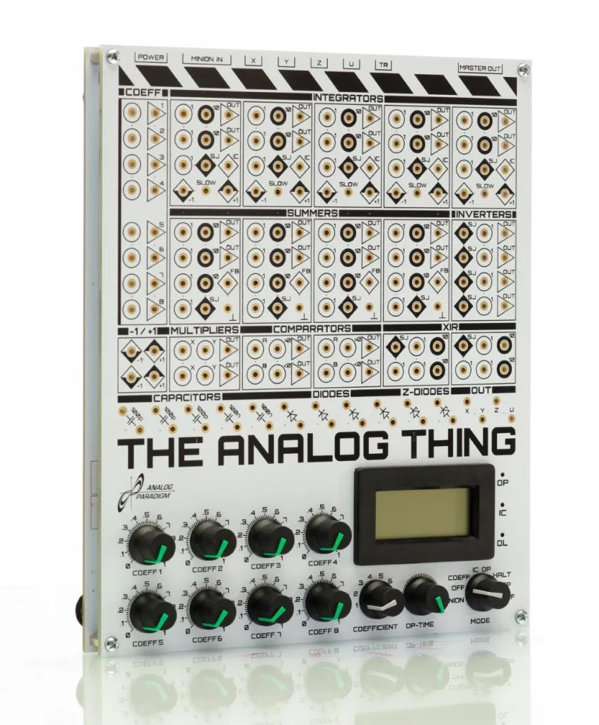
Figure 2 — THAT v1.3 front panel. The coefficient potentiometers (COEFF1–8) occupy the right strip; mode selector, OP-time pot, and coefficient selector are at lower right. Integrators INT1–INT5 run across the upper left; summers SUM1–SUM4 occupy the middle band. Output jacks X, Y, Z, U are visible at upper right.
4.7 Full Worked Example — Damped Harmonic Oscillator
This section demonstrates the complete programming workflow: equation → patch diagram → magnitude scaling → time scaling → coefficient setting → display. The system chosen — a damped harmonic oscillator — is fundamental to mechanics, acoustics, and electronics, and it exercises two integrators, one summer, two coefficient potentiometers, and the comparator (optionally, for detecting zero-crossings).
4.7.1 Physical system
A mass m on a spring with stiffness s and viscous damping coefficient D, displaced from equilibrium:
$$m\ddot{y} + D\dot{y} + sy = 0$$
Dividing by m and isolating the highest derivative:
$$\ddot{y} = -\frac{D}{m}\dot{y} - \frac{s}{m}y$$
Define for brevity: α = D/m, β = s/m.
$$\ddot{y} = -\alpha\dot{y} - \beta y$$
Characteristic angular frequency ω₀ = √β, damping ratio ζ = α/(2ω₀).
Representative numerical values (from the First Steps mass-spring-damper example):
- s = 0.5 (spring coefficient, pot 2)
- D = 0.05 (damping coefficient, pot 3)
- 1/m = 0.5 (inverse mass, pot 4)
- y₀ = 0.5 (initial displacement, pot 1)
4.7.2 Step 1 — Magnitude scaling
Identify peak excursions. For underdamped motion, y oscillates with amplitude ≈ y₀ at start. Velocity peak ≈ ω₀ × y₀. With β = s/m = 0.5 × 0.5 = 0.25, ω₀ = 0.5 rad/ms. At y₀ = 0.5 MU, velocity peak ≈ 0.25 MU. Both are well within ±1 MU — no additional scaling is needed for these values. Acceleration peak ≈ β × y₀ = 0.125 MU. All nodes are comfortably below the 0.9 MU design ceiling.
4.7.3 Step 2 — Time scaling
The natural period is T = 2π/ω₀ = 2π/0.5 ≈ 12.6 ms. In REPF mode at 80 ms OP time, the patch traces approximately six full oscillation cycles — adequate for observing the decay envelope. No time scaling beyond the coefficient choices is required.
4.7.4 Step 3 — Patch diagram
The signal-flow diagram below shows the complete patch. Sign tracking is annotated at each node.
                          α (COEFF3)      β (COEFF2)
                             │                │
  ┌──────────────────────────┴────────────────┴──────┐
  │                                                   │
  │         SUM1 (×1 inputs)                         │
  │   −ẏ ──────────────────────────►                 │
  │    y ───────────────────────────►  −ÿ ───────────┤
  │                                         │         │
  └─────────────────────────────────────────┘         │
                                                      │
   COEFF1 (y₀) → IC                                   │
   +1 ─[COEFF1]─► IC jack of INT1                    │
                                                      ▼
            ┌────────────────────────────────[SUM1 output]
            │                                         │
           INT1 (fast) ◄── IC = −y₀                  │
            │                                         │
            │  output = +ẏ (inverted of −ẏ)           │
            ▼                                         │
           INT2 (fast) ◄── IC = 0                    │
            │                                         │
            │  output = −y (inverted of +ẏ)           │
            │                                         │
           INV1 ──► y (positive displacement)         │
            │                                         │
            ├──────────────────────────────────────►  │ (via COEFF2 = β)
            │                                         │
            └── to OUT X (display)                    │
                                                      │
  INT1 output (+ẏ) ──[INV2]──► −ẏ ──► SUM1 (via COEFF3 = α)
Figure 3 — Signal-flow patch for damped harmonic oscillator (THAT v1.3)
4.7.4.1 Patch diagram — SVG format
Figure 4 — SVG signal-flow diagram for damped harmonic oscillator on THAT
4.7.5 Step 4 — Front-panel patching procedure (step by step)
- Set THAT to COEFF mode.
- Set COEFF1 = 0.5 (initial displacement y₀). Output will drive IC of INT1 (inverted by INT1 → IC input delivers −y₀, so INT1 output starts at +y₀ = +0.5 MU after IC phase).
- Set COEFF2 = 0.5 (spring coefficient β = s/m).
- Set COEFF3 = 0.05 (damping coefficient α = D/m).
- Patch cables — switch to IC mode first, then make connections:
Table 9 — Step 4 — Front-panel patching procedure (step by step)
| From | To | Purpose |
|---|---|---|
| COEFF1 output | INT1 IC jack | Sets initial displacement |
| INT1 output | INT2 input (×1) | Chains integrators: ẏ → y |
| INT2 output | INV1 input | Recover sign: −y → +y |
| INV1 output | OUT X jack | Route +y to oscilloscope |
| INT1 output | INV2 input | Tap ẏ for damping term |
| INV2 output | SUM1 input 1 (×1) | −ẏ to summer |
| INT2 output | COEFF3 input | −y scaled by α |
| COEFF3 output | SUM1 input 2 (×1) | −αy to summer |
| INV1 output | COEFF2 input | +y scaled by β |
| COEFF2 output | SUM1 input 3 (×1) | +βy — but need −βy! |
| SUM1 output | INT1 input (×1) | Feedback closes loop |
Table 9 — Cable connections for damped harmonic oscillator
Note — The summer SUM1 itself inverts its output sum. If −ẏ and −αy enter SUM1 on ×1 inputs and +βy also enters SUM1, the summer output equals −(−ẏ − αy + βy) = ẏ + αy − βy. This is incorrect. The correct approach: feed −y (direct INT2 output, before INV1) into COEFF2, so SUM1 receives −ẏ and −βy and −αy, and SUM1 inverts to give +ẏ + βy + αy. Because INT1 inverts its input, INT1 sees −(ẏ + βy + αy) = −ẏ − βy − αy, which after integration gives − ∫(ẏ + βy + αy) — correct. Sign bookkeeping is critical; trace every inversion.
-
Switch to OP mode (or REP/REPF for repetitive display). The oscilloscope connected to X should display a decaying sinusoid for underdamped conditions (α < 2√β) or an exponential decay for overdamped.
-
Interactive parameter exploration: With the patch running in REPF at 80 ms, rotate COEFF2 (spring) and COEFF3 (damping) while observing the display. Increasing COEFF3 toward critical damping (α = 2√β) causes oscillations to vanish and the output to approach equilibrium monotonically.
4.7.6 Step 5 — Magnitude scaling verification
With y₀ = 0.5 MU and the parameter values above, the computed peak values are:
Table 10 — With y₀ = 0.5 MU and the parameter values above, the computed peak values are
| Node | Expression | Peak value (MU) | Within ±0.9 MU? |
|---|---|---|---|
| y (displacement) | INT2 output after INV | 0.50 | Yes |
| ẏ (velocity) | INT1 output | ≈ 0.25 | Yes |
| ÿ (acceleration, SUM1) | ≈ β×y + α×ẏ | ≈ 0.26 | Yes |
Table 10 — Node peak excursion check for worked example
All nodes are well within the 0.9 MU ceiling. If y₀ were set to 0.95, the acceleration node would approach 0.5 MU — still safe. Only if y₀ approached 1.0 and an external forcing term were added would overload become a concern.
4.7.7 Step 6 — Displaying results
- Time domain: Connect OUT X to oscilloscope Ch1. Select REP mode, OP time = 2 s. Set oscilloscope to roll mode at 200 ms/div. Observe decaying sinusoid in real time.
- Phase plane (ẏ vs y): Patch INT1 output (ẏ) to OUT Y. Select REPF mode, OP time = 80 ms. Set oscilloscope to X-Y mode. The display shows a spiral trajectory converging to the origin — a phase portrait of the damped oscillator.
- Coefficient monitoring: Patch INT2 output (or INV1 output) to U jack. Panel meter reads instantaneous y in IC, OP, and HALT modes.
4.7.8 Expected results
  Time-domain output (underdamped, ζ ≈ 0.05):

    +1 ┤
  0.5 ┤   ╭──╮        ╭──╮
       ┤  ╭╯  ╰──╮  ╭─╯  ╰──╮
       ┤ ─╯      ╰──╯        ╰────────
  0.0 ┤─────────────────────────────────────► t
       ┤
  −0.5┤
    −1 ┤

  Phase-plane output (spiral converging to origin):

         ẏ
    ┤  ↗ ○ ↘
    ┤ ↑   │  ↓
    ┤ ←   0  →    y
    ┤ ↑   │  ↓
    ┤  ↖ ○ ↙      (spiral inward over successive cycles)
Figure 5 — Schematic expected output for damped oscillator (underdamped case)
4.8 Reference — Jack and Color Conventions
The First Steps guide and standard analog computing practice use consistent visual conventions for patch diagrams. The table below codifies these for THAT.
Table 11 — Reference — Jack and Color Conventions
| Jack marking | Shape | Meaning |
|---|---|---|
| White circle + “1” | ○₁ | Input, weight ×1 |
| Black circle + “10” | ●₁₀ | Input, weight ×10 |
| Triangle | ▷ | Output |
| White diamond + “+1” | ◇⁺ | Machine unit +1 source |
| Black diamond + “−1” | ◆⁻ | Machine unit −1 source |
| White diamond + “IC” | ◇ᴵᶜ | Initial condition input |
| White diamond + “FB” | ◇ᶠᴮ | Feedback resistor jumper (summers) |
| White diamond + “SLOW” | ◇ˢ | SLOW mode connection (integrators) |
| Ground symbol | ⏚ | THAT chassis ground (summers) |
| SJ | — | Summing junction (for XIR chaining) |
Table 11 — Jack symbols and meanings on THAT patch panel
4.8.1 Patch cable color conventions (informal community standard)
THAT ships with 30 patch cables in a mixed set. The First Steps manual does not mandate specific colors for signal types, but the following conventions appear consistently in anabrid documentation:
Table 12 — signal types, but the following conventions appear consistently in anabrid documentation
| Suggested color | Typical use |
|---|---|
| Red | Highest derivative / feedback |
| Blue | Integrated signals (state variables) |
| Green | Display outputs |
| Yellow | Coefficient potentiometer connections |
| Black | Ground, IC connections |
| White | Machine unit (+1/−1) sources |
Table 12 — Informal patch cable color conventions (community practice)
4.9 Newsletter Reference Table
The 16 issues of THE ANALOG THING Newsletter (anabrid GmbH, 2021–2023) document the development history and community applications of THAT. Issues relevant to programming technique include:
Table 13 — and community applications of THAT. Issues relevant to programming technique include
| Issue | Date | Programming/application content |
|---|---|---|
| #1 | 2021-09-30 | Hindmarsh-Rose neuron model; introduction of HYBRID port |
| #2 | 2021-11-27 | Hybrid computer coupling (Arduino Mega); exponential mapped past |
| #3 | 2022-01-17 | Euler spiral (all 5 integrators in use) |
| #4 | 2022-03-03 | First Steps booklet released; Rössler attractor on two THATs |
| #7 | 2022-05-16 | Four-quadrant division; polynomial generator community posts |
| #8 | 2022-06-16 | Chirp / gravitational wave on two THATs; TeensyScope |
| #10 | 2022-08-24 | THE HYBRID THING; VCF Euler spiral demo |
| #11 | 2022-09-19 | Bessel functions; quantum two-body problem; polynomial display |
| #16 | 2023-09-xx | Koch’s THAT Analog Computer Book released |
Table 13 — Newsletter index: programming and application content
4.10 Cross-Reference to Other Volumes
- Vol 1 — Overview & the modern-analog revival: History, context, Anabrid, open-hardware ethos.
- Vol 2 — Hardware & architecture: Detailed op-amp topology of integrators, summers, multipliers, comparators.
- Vol 3 — Computing elements & patching: Jack types, resistor networks, SJ jacks, SLOW jacks, diodes, capacitors.
- Vol 5 — Worked examples & applications: Lorenz, pendulum, predator-prey, and other patch walkthroughs.
- Vol 6 — Expansion & hybrid: HYBRID port protocol, Arduino/Raspberry Pi interfacing, REPF synchronisation, master/minion chaining.
Key takeaway — The programming discipline for THAT reduces to four steps applied in order: (1) isolate the highest derivative; (2) chain integrators to build the state-variable ladder; (3) scale magnitudes so no node exceeds ±0.9 MU; (4) choose operating speed via SLOW jacks or time-scaled coefficients and select REP/REPF for the desired display mode. Everything else — multiple equations, nonlinear terms from multipliers, conditional switching from comparators — is an extension of this core workflow.
Comments (0)