THAT — The Analog Thing · Volume 3
THE Analog Thing — Volume 3 — Computing elements & patching
Element-by-element reference for THAT's patch field: integrators, summers, multipliers, comparators, coefficient pots, and the +/−10 V machine-unit convention
3.1 About this Volume
This volume is the working desk reference for anyone who needs to know what every computing element on THAT does, how many of each type the machine provides, what the input-weighting scheme means electrically, and how the 2 mm banana-jack patch system operates. Volumes 1 and 2 cover the hardware architecture and power/signal infrastructure; Volume 4 covers problem scaling and time scaling in depth; Volume 5 treats the HYBRID port and master/minion chaining. This volume assumes familiarity with operational-amplifier theory at the level of a senior EE (inverting integrator, virtual-ground summing node) and focuses instead on the THAT-specific details: exact jack assignments, weighting conventions, mode sequencing, and practical patching discipline.
All element counts and electrical values stated here are verified from two independent sources: the First Steps v2.0 manual (Fischer & Ulmann, anabrid GmbH, 2023) and the v1.3 schematics released publicly by Analog Paradigm / anabrid GmbH on GitHub (THAT-Front_v1.3_01.png, THAT-Front_v1.3_02.png, and THAT-Base_v1.3_01 through _05). Where a value appears in only one source, that source is cited explicitly.
Note — The schematic set is labeled v1.3 (March 2022). All element counts and signal assignments documented here reflect that revision, which is the production standard at time of writing. Earlier prototypes differed in minor details (e.g., the absence of the HYBRID port in v1.0 boards).
3.1.1 Element Inventory at a Glance
Before diving into per-element detail, the complete functional inventory of the THAT patch field is presented here for orientation. All counts are derived from the v1.3 schematics; the corresponding First Steps references are cited in the per-element sections below.
3.1.2 Anatomy of a THAT Patch
Every analog computation on THAT reduces to the same four-step structure:
- State variables — held in integrators, their outputs representing the solution quantities.
- Arithmetic — summers and multipliers compute the right-hand sides of the governing ODEs.
- Conditioning — coefficient pots scale terms; comparators implement switching conditions.
- Feedback — integrator outputs are routed back as inputs, closing the ODE loop.
The machine-unit rail (±1, physically ±10 V) supplies bias voltages and initial conditions. Passive elements (diodes, capacitors) handle nonlinear shaping and energy storage in specialized patches. Everything is wired with 2 mm banana-plug cables into the 186-position patch field.
3.2 Integrators
3.2.1 Count and Identification
THAT provides five integrators, labeled INT1 through INT5 on the front PCB schematic. This is verified directly from THAT-Front_v1.3_02.png, which shows five distinct integrator blocks: INT1, INT2, INT3 in the upper row and INT4, INT5 in the lower row (with SUM1 beginning the summer group in that row). The five integrators represent the single largest functional block on the panel.
Note — The First Steps manual confirms five integrators indirectly: Newsletter #3 (2022-01-17) notes “a program [that] makes full use of the five integrators on THAT” in the context of the Euler-spiral application; the Euler-spiral patch diagram in section 9.5 of the manual uses all five integrators simultaneously. The schematic count of five is the primary authority.
3.2.2 Op-amp Implementation
Each integrator is built around a TL074H quad JFET op-amp (the production standard, confirmed from Newsletter #9 and the schematics). The TL074H is a precision quad op-amp with JFET inputs, low input bias current, and low offset voltage — all of which directly benefit integrator accuracy by reducing charge leakage from the feedback capacitor during HALT or IC hold. The feedback element is a capacitor — the classic Miller integrator topology. The output is taken from the inverting output of the op-amp, which means THAT’s integrators implicitly invert sign: if the input is a positive-going signal, the output ramps negative. This inversion is a fundamental property that must be accounted for in every patch.
The integration time constant τ = RC, where R is the input resistor value (setting the weight of 1 for ×1 inputs, R/10 effective for ×10 inputs) and C is the feedback capacitor. THAT provides a SLOW jack on each integrator: connecting an integrator’s output to its own SLOW jack engages an additional capacitor in parallel with the feedback capacitor, increasing the effective C and therefore the time constant by a factor of 100 (×0.01 speed). The First Steps manual (§8) states: “in the slow operation mode, the input of −1 and a run beginning at IC=0 lead to the output of +1 in 100 ms” — versus 1 ms at normal speed. This 100× slowdown is useful for simulating slow phenomena at human-observable speeds without recalculating coefficient values.
3.2.3 Input Structure
Each integrator exposes five weighted input jacks plus one initial-condition jack:
Table 1 — Each integrator exposes five weighted input jacks plus one initial-condition jack
| Jack label | Symbol on panel | Weight factor | Physical circle color |
|---|---|---|---|
| Input 1 | 1 (×3) | ×1 | White |
| Input 2 | 10 (×2) | ×10 | Black |
| IC | diamond outline | — (sets initial state) | White diamond |
The three unity-weight inputs and two ×10 inputs are summed at the virtual-ground summing junction (SJ) before the integrating capacitor. A signal of value −0.02 machine units applied to a ×10 input produces an effective input contribution of −0.2 machine units — exactly as for the analogous summer inputs (see §3).
Tip — The ×10 inputs are valuable when a scaled signal is naturally small. Feeding a coefficient-potentiometer output (range 0 to +1) into a ×10 input and setting the pot to 0.05 achieves an effective coefficient of 0.5 without requiring a separate multiplication stage.
3.2.4 Output Jacks
Each integrator provides two output jacks (INT-Out1 and INT-Out2 in the schematic, labeled with triangle symbols on the panel). Both carry the same signal. Providing two output jacks allows the output to fan out to two destinations without stacking banana plugs, though stacking is permitted for additional fan-out.
3.2.5 Initial Condition (IC) Jack and IC Mode
The IC jack accepts an external voltage that defines the integrator’s output value at the moment THAT transitions from IC mode to OP mode. Internally the IC is applied with inversion: the integrator output in IC mode equals the negative of the voltage applied to the IC jack. If the IC jack is left unpatched the initial condition defaults to zero.
        IC jack (white diamond)
             |
             ▼
         ┌───────────────────────────────┐
         │  ×1  ×1  ×1  ×10  ×10        │
  x1 ─○──┤  R   R   R    R    R          │
  x1 ─○──┤       Σ at SJ                 │──C──┐──▷ OUT1
  x1 ─○──┤         │                     │     │──▷ OUT2
 x10 ─●──┤         ▼                     │     │
 x10 ─●──┤       [−∫ dt]                 │◄────┘
         │                               │
         │  SLOW jack: extra C in loop   │
         └───────────────────────────────┘
          ○ = white circle (×1)  ● = black circle (×10)
3.2.6 Operational Modes Affecting Integrators
Table 2 — Operational Modes Affecting Integrators
| Mode | Integrator behavior |
|---|---|
| IC | Output driven to −(IC jack voltage); capacitor held charged to that value |
| OP | Normal integration; output evolves according to weighted input sum |
| HALT | Integration suspended; output held at last value (capacitor isolated) |
| REP | Automatic IC → OP → IC cycling at OP-Time Potentiometer rate (0–10 s) |
| REPF | Same as REP but 100× faster (0–100 ms per cycle) |
| MINION | Integrator control handed to master THAT via ribbon cable |
| COEFF | Integrators idle; panel meter reads selected coefficient pot |
Note — In HALT mode the output voltage is held by the charge trapped on the feedback capacitor. Leakage current in the op-amp input stage will cause slow drift; HALT is intended for short pauses, not extended holds. For truly static holds, switch to MINION mode with no master clock active.
3.3 Summers
3.3.1 Count and Identification
THAT provides four summers, labeled SUM1 through SUM4 on the front PCB schematic (THAT-Front_v1.3_02.png). SUM1 shares the upper section of the panel with the integrators; SUM2, SUM3, SUM4 are in the lower-middle region.
3.3.2 Input Structure
Each summer exposes seven weighted input jacks:
Table 3 — Each summer exposes seven weighted input jacks
| Jack type | Count | Weight | Panel symbol |
|---|---|---|---|
| Unity-weight inputs | 4 | ×1 | White circles labeled 1 |
| Ten-weight inputs | 3 | ×10 | Black circles labeled 10 |
| Total inputs | 7 | — | — |
This is a larger input count than any single integrator, making summers the natural aggregation points for multi-term differential equation components.
Like the integrators, summers are built around inverting op-amp summing junctions and implicitly invert the sign of the weighted sum. The output is:
$$y = -\left(\sum_{i=1}^{4} x_{1,i} + 10 \cdot \sum_{j=1}^{3} x_{10,j}\right)$$
(all values in machine units)
3.3.3 Output Jacks
Each summer provides two output jacks (SUM-Out1 and SUM-Out2) carrying identical signals, for the same fan-out rationale as the integrators.
3.3.4 Feedback (FB) and Ground Jacks
Each summer provides two special jacks not present on integrators:
- FB jack (white diamond): A feedback path jack that connects a signal directly into the summing junction from outside. This is used to close a feedback loop around a summer without the feedback resistor attenuating the signal, enabling high-gain or comparator-like configurations.
- Ground jack (symbol
⏚): Exposes THAT’s analog ground. Combined with the FB jack this allows zero-crossing-detection configurations using the summer as an amplifier with feedback.
3.3.5 Summing-Junction (SJ) Extension
Each summer (like each integrator and inverter) carries an SJ jack. Connecting the SJ jack of a resistor-network module (XIR) to the SJ jack of a summer electrically parallels the XIR’s input resistors onto the summer’s virtual-ground node, adding up to two more ×1-weighted inputs without degrading the summer’s gain accuracy. THAT provides two XIR modules (XIR1 and XIR2 visible in THAT-Front_v1.3_01.png).
SUM block diagram:

  ×1 ─○──R─┐
  ×1 ─○──R─┤
  ×1 ─○──R─┤ (SJ)──┬──[−A]──┬──▷ SUM-Out1
  ×1 ─○──R─┤       │        └──▷ SUM-Out2
 ×10 ─●──R─┤  ◄─── FB jack
 ×10 ─●──R─┤
 ×10 ─●──R─┘
  XIR SJ ──(optional extension)
  ⏚ jack = analog GND reference
3.4 Inverters
3.4.1 Count and Identification
THAT provides four inverters, labeled INV1, INV2, INV3, and INV4 on the front PCB schematic. The schematic (THAT-Front_v1.3_02.png) groups them as INV1/2 and INV3/4 in paired blocks at the lower-left of the front panel, each block sharing a physical IC package. The First Steps manual (Section 7, item 8) describes them tersely: “Inverters yield the input value with the opposite sign.”
Four inverters are provided because sign inversion is the most frequently needed single-element operation in analog computing. Every integrator and summer already inverts implicitly, but a standalone inverter corrects the sign of a signal without adding weighted integration or summation to the signal path.
3.4.2 Input Structure
Each inverter exposes two unity-weight input jacks (×1). Unlike integrators and summers, inverters provide no ×10 inputs. The output is:
$$y = -(x_1 + x_2)$$
With only x₁ connected: y = −x₁ (simple sign inversion). With both inputs connected: y = −(x₁ + x₂) (sign-inverting two-input summer). This makes each inverter usable as a two-input inverting summer when the full output flexibility of a SUM block is not needed.
3.4.3 Output and SJ Jacks
Each inverter provides two output jacks carrying identical inverted signals. Each inverter also carries an SJ (Summing Junction) jack, allowing a resistor network (XIR) to be attached to add additional ×1-weighted inputs.
3.4.4 Inverter Specifications
Table 4 — Inverter Specifications
| Parameter | Value | Source |
|---|---|---|
| Count | 4 | Schematic THAT-Front_v1.3_02.png |
| ×1 inputs per unit | 2 | Schematic; First Steps §8 |
| ×10 inputs | None | Schematic |
| Output jacks | 2 per unit | Schematic |
| SJ jack | 1 per unit | First Steps §8 |
| Sign convention | Inverting | First Steps §7 item 8 |
3.4.5 Role in Patches
Inverters address a fundamental sign-management challenge in analog computing: because every integrator and summer implicitly inverts, patches with even numbers of elements in a loop accumulate a double inversion (net positive gain), which can cause the loop to be non-negative-feedback and diverge. Keeping track of inversions and inserting a standalone inverter to correct the sign is standard practice.
Sign inversion budget example — second-order oscillator:

  ẍ = −ω²x

  INT1: integrates ẋ → x (inverts: output = −∫ẋ dt = x if ẋ correctly signed)
  INT2: integrates ẍ → ẋ (inverts again)
  After two integrators: two inversions cancel → net: x available at INT2 output

  Feedback of x to INT2 input (which takes −ẍ):
    Need: input to INT2 = +ω²x
    INT2 is inverting, so: output = −∫(ω²x)dt = −ẋ   ← correct if x is positive-going

  No standalone inverter needed for this specific loop.
  But displaying x requires INT1 output, which is −x.
  Solution: route INT1 output through INV1 before OUT X.
Tip — Before starting any patch, draw the sign at every node in the patch diagram. Count the number of inversions around each feedback loop. An odd total means the loop is negative (stabilizing); an even total means it is positive (unstable/diverging) unless the patch is intentionally designing a relaxation oscillator or hysteresis circuit. Use inverters to correct the count as needed.
3.5 Multipliers
3.5.1 Count and Identification
THAT provides two multipliers, labeled MUL1 and MUL2 on the base PCB schematic (THAT-Base_v1.3_04.png). The schematic shows two distinct four-quadrant multiplier stages (MUL-X and MUL-Y subblocks) for each channel, implemented with the AD633-type topology using two op-amp stages visible in the schematic.
Note — The First Steps manual (Section 7, item 20) states only “Multipliers multiply values supplied to their inputs” without specifying the count in a standalone sentence. The count of two is read directly from the schematic labels MUL1/2 visible in
THAT-Base_v1.3_04.png. The front-panel reference in the annotated panel diagram (item 20) labels a single region “Multipliers”, consistent with two units side by side.
3.5.2 Functional Description
Each multiplier computes the continuous-time product of two input signals and delivers the result scaled to machine units:
$$z = x \cdot y \quad \text{(in machine units)}$$
Both inputs accept the full machine-unit range (−1 to +1, i.e., −10 V to +10 V). The output is likewise bounded to ±1 machine unit. Both inputs must stay within machine-unit limits or the output will be clamped or distorted.
Four-quadrant operation means all sign combinations are valid:
Table 5 — Four-quadrant operation means all sign combinations are valid
| x sign | y sign | z sign |
|---|---|---|
| + | + | + |
| + | − | − |
| − | + | − |
| − | − | + |
3.5.3 Input/Output Jacks
Each multiplier exposes:
Table 6 — Each multiplier exposes
| Jack | Count | Description |
|---|---|---|
| MUL-A1, MUL-A2 | 2 | X-input jacks (both deliver same input) |
| MUL-B1, MUL-B2 | 2 | Y-input jacks |
| MUL-OUT1, MUL-OUT2 | 2 | Output jacks (identical signal) |
The dual input jacks allow stacking a second patch cable without mechanical conflict and provide a convenient fan-in for the same signal.
3.5.4 Practical Use
Multipliers are the highest-cost elements on THAT in terms of patch complexity: they consume two input channels instead of one and are used when nonlinear terms appear in the governing equations. Common uses:
- Squaring a signal: patch the same output to both multiplier inputs (x² term in polynomial, centripetal force).
- Cross-product terms: Lorenz attractor requires σ·z and x·y products — two multipliers are needed simultaneously.
- Amplitude modulation: one input carries a carrier, the other a modulating envelope.
Tip — When only one multiplier is available and the patch requires x², the squarer configuration (self-patch) frees the second multiplier for another term. With only two multipliers, the Lorenz attractor (which needs both) consumes the entire multiplier budget; patches requiring three multiplications must resort to master/minion chaining (see Vol 5).
3.6 Comparators
3.6.1 Count and Identification
THAT provides two comparators, labeled CMP1 and CMP2 on both the base schematic (THAT-Base_v1.3_04.png) and the front-panel schematic (THAT-Front_v1.3_01.png). The schematic shows each comparator as a two-stage circuit: a summing node followed by a fast comparator IC and then an output buffer.
3.6.2 Functional Description and Circuit
Each comparator implements a conditional signal router — an analog multiplexer with a zero-crossing threshold. The First Steps manual (Section 7, item 21) states:
“If A+B > 0, then the input to
>is available at the two output jacks, otherwise the input to<is available at the two output jacks.”
This describes a two-input analog switch controlled by the algebraic sum of two control signals (A and B). The switching threshold is zero (i.e., the midpoint of the machine-unit range).
The comparator introduces a small propagation delay (the switching time of the comparator IC and buffer), but for the continuous-time signals typical of THAT patches this delay is negligible.
3.6.3 Jack Summary
Table 7 — Jack Summary
| Jack | Role |
|---|---|
| CMP-A | Control input A |
| CMP-B | Control input B |
| CMP->_IN | Signal to route when A+B > 0 |
| CMP-<_IN | Signal to route when A+B ≤ 0 |
| CMP-OUT1 | Output (selected signal), copy 1 |
| CMP-OUT2 | Output (selected signal), copy 2 |
3.6.4 Practical Use
Comparators enable piecewise-linear and switched-parameter patches — the closest THAT gets to conditional logic. Representative applications from the First Steps manual:
- Bouncing ball (section 9.8): a Zener diode in series with comparator action detects when the ball’s y-position crosses zero (the floor) and injects a velocity reversal impulse.
- max(A, B) / min(A, B) helper functions (sections 10.1, 10.2): the comparator routes whichever of two inputs is larger/smaller to the output.
- abs(A) helper function (section 10.3): comparator selects between +A and −A depending on sign.
- Non-negative clamp (section 10.5): comparator routes A when positive, zero otherwise.
3.7 Coefficient Potentiometers
3.7.1 Count and Identification
THAT provides eight coefficient potentiometers, labeled PT1 through PT8 (also referred to as COEFF1 through COEFF8 in the base schematic, region COEFF1-8 visible in THAT-Front_v1.3_01.png). The First Steps manual (Section 7, item 17) refers to “Coefficient Potentiometers” and item 23 labels the associated jacks “Coefficients.” Newsletter #4 explicitly references “the eight coefficient potentiometers” during a description of the test procedure.
Each potentiometer is a single-turn wirewound or cermet pot (production hardware uses a smooth, gradual scale rather than the numbered scale of the very first prototypes, a change noted in Newsletter #1).
3.7.2 Electrical Function
Each coefficient potentiometer is a voltage divider. When its input jack is connected to the +1 machine-unit supply, the output jack delivers a continuously adjustable voltage in the range 0 to +1 (0 V to +10 V). The pot’s wiper position controls the fraction.
To obtain a signed coefficient in the range −1 to +1, the adjustable value helper function (section 10.4 of First Steps) is used: it combines +1 and −1 machine-unit supplies with a comparator to produce a pot-controllable output spanning the full bipolar range.
Table 8 — Electrical Function
| Pot input connected to | Output range |
|---|---|
| +1 machine unit | 0 to +1 (unipolar positive) |
| −1 machine unit | −1 to 0 (unipolar negative) |
| Helper function ±1 circuit | −1 to +1 (bipolar) |
3.7.3 Setting Procedure
- Connect the desired pot’s input jack to the +1 machine-unit supply.
- Place the Mode Selector in COEFF mode.
- Turn the Coefficient Selector knob to select the desired potentiometer (PT1–PT8).
- Observe the Panel Meter, which reads 0–1 in COEFF mode.
- Adjust the pot knob until the displayed value matches the desired coefficient.
- Repeat for each potentiometer used in the patch.
Note — In COEFF mode the integrators are idle. Setting all coefficients before entering IC or OP mode is the standard workflow.
3.7.4 Jack Assignments
Table 9 — Jack Assignments
| Pot identifier | Input jack label | Output jack label |
|---|---|---|
| PT1 | PT1-IN | PT1-OUT |
| PT2 | PT2-IN | PT2-OUT |
| … | … | … |
| PT8 | PT8-IN | PT8-OUT |
(Naming convention from the base PCB schematic THAT-Base_v1.3_02.png, which shows PT1-IN through PT8-IN and corresponding -OUT lines driving the front-panel coefficient section.)
The Coefficient Selector routes one potentiometer output to the Panel Meter at a time; all eight output jacks remain live simultaneously regardless of the selector position.
3.8 The Patching System
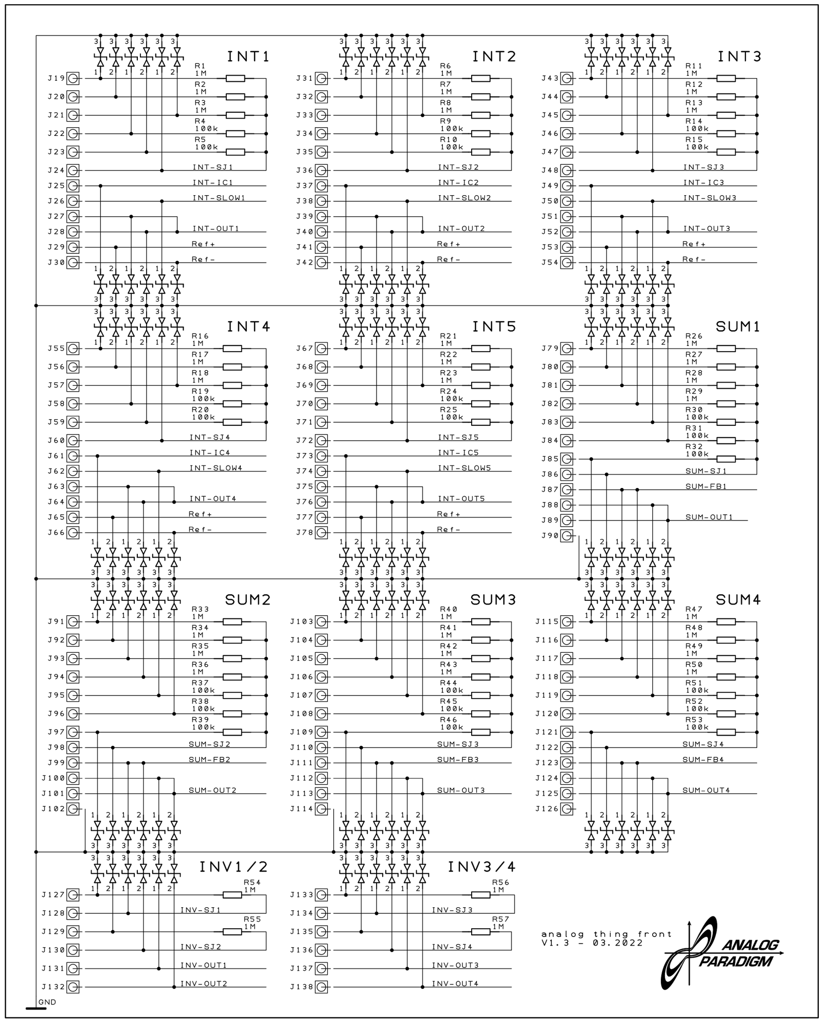
Figure: THAT v1.3 front panel schematic showing the full jack layout across the patch field. Reading top-to-bottom: integrators (INT1–INT5), summers (SUM1–SUM4), inverters (INV1–INV4), resistor networks (XIR1–2) at upper left; coefficient potentiometers (COEFF1–8) at upper right; multipliers and comparators in the lower base schematic region.
3.8.1 Physical Format: 2 mm Banana Jacks
THAT’s patch field uses 2 mm banana-plug patch cables — a format distinct from the 4 mm banana plugs common in laboratory instruments and from the 3.5 mm mini-jack format of modular synthesizers. The 2 mm format was chosen deliberately: smaller than 4 mm (allowing higher jack density on the panel) and more rugged than spring-clip patchbay formats used on historic Telefunken and EAI analog computers. The cables supplied with THAT are single-wire (one conductor, no shield), which is adequate because the patch signals are low-impedance op-amp outputs with source impedances of tens of ohms driving loads of tens of kilohms.
The patch field uses gold-plated through-holes in an extra-thick PCB rather than conventional socket hardware. This design reduces per-position cost significantly — the First Steps FAQ (section 11) notes that a conventional socket would cost approximately USD 1.00 each, which across 186 positions would add roughly USD 186 to the bill of materials. The through-hole approach means plugs do not fully seat; the contact spring at the midpoint of the plug barrel makes reliable electrical contact at the gold-plated barrel wall. Plugs may be stacked (inserted into the same hole atop each other) to fan a single output to multiple inputs.
Note — The gold-plated through-holes can accumulate conductive contamination from finger contact (skin oils, flux residue). The First Steps FAQ notes that this is the primary cause of integrators running into overload unexpectedly. A gentle clean with isopropyl alcohol on a cotton swab resolves this. Do not use abrasive materials.
3.8.2 Jack Count: 186 Positions
The total number of plug positions on the patch panel is 186, confirmed by the First Steps FAQ: “one of these sockets plus mounting costs about USD 1.00, which would add up significantly for the 186 plug positions on THAT’s patch panel.” This figure encompasses all input jacks, output jacks, IC jacks, SJ jacks, machine-unit jacks, diode jacks, capacitor jacks, and output-selector jacks.
3.8.3 Jack Shape Vocabulary
Table 10 — Jack Shape Vocabulary
| Shape | Fill | Meaning |
|---|---|---|
Circle ○ | White | Input, unity weight (×1) |
Circle ● | Black | Input, ten weight (×10) |
Triangle ▷ | — | Output |
Diamond ◇ (upper black) | Black top / white bottom | Machine unit +1 source |
Diamond ◇ (lower black) | White top / black bottom | Machine unit −1 source |
Diamond ◇ (all white) | White | IC or FB jack (special function) |
3.8.4 Signal Direction Rules
These rules must never be violated:
- One driver per jack: an input jack may receive exactly one patch cable. Connecting two outputs to the same input jack shorts two op-amp output stages together — a fault condition that triggers the overload LED (OL) and may cause thermal damage to the op-amp output stage.
- Outputs may fan out freely: one output jack may be connected to any number of input jacks by stacking cables or by daisy-chaining through multiple input jacks.
- No output-to-output connections: the patch panel provides no protection against this; the operator must prevent it.
- Do not connect +1 to ground: the First Steps FAQ explicitly warns that connecting the +1 machine-unit supply to ground will blank the display (as it causes a short on the ±10 V reference).
Tip — If a node must drive more than two or three destinations and stacking feels unwieldy, route the signal through a spare unity-weight summer input (with all other inputs unpatched) to create a buffered copy. The inverting sign of the summer must then be cancelled by another inverter — or accounted for in the patch algebra.
3.8.5 Patch Field Jack-Type Decision Tree
Given a jack position on the panel — how to identify it:

Is the symbol a TRIANGLE?
  YES → Output jack. May drive any number of inputs (stack cables freely).
  NO  → Is it a CIRCLE?
          YES → White circle with "1"? → Unity-weight input (×1).
                Black circle with "10"? → Ten-weight input (×10).
          NO  → Is it a DIAMOND?
                  Upper half black? → Machine-unit +1 source (+10 V).
                  Lower half black? → Machine-unit −1 source (−10 V).
                  All white?        → IC jack (integrator) or FB jack (summer).
                Is it labeled "SJ"? → Summing Junction extension point.
                Is it labeled "⏚"? → Analog ground reference.
3.8.6 Daisy-Chaining and Fan-Out Table
Table 11 — Daisy-Chaining and Fan-Out Table
| Fan-out need | Recommended method | Notes |
|---|---|---|
| 1 → 2 destinations | Use both output jacks (OUT1, OUT2) | All elements provide 2 outputs |
| 1 → 3 destinations | Stack a cable in OUT1 or OUT2 | Spring contact is rated for stacking |
| 1 → 4+ destinations | Stack multiple cables or route through buffer summer | Consider signal loading |
| Signal inversion needed | Route through inverter (INV1–INV4) | Each inverter: 2×(×1) inputs, 2 outputs |
| Signal with gain scaling | Route through summer with ×10 input, or through coeff pot | Pot range 0–1 limits unity gain |
3.8.7 The +/−10 V Machine-Unit Convention
THAT represents all computed quantities as voltages in the range −10 V to +10 V. This range is called the machine unit, abstractly normalized to −1 to +1. The +10 V and −10 V supply rails are derived from a DC/DC converter that steps the 5 V USB input up to ±12 V, from which precision ±10 V references are generated for the machine-unit jacks on the panel.
Table 12 — The +/−10 V Machine-Unit Convention
| Abstract value | Physical voltage | Machine-unit jack |
|---|---|---|
| +1 | +10 V | +1 (upper-black diamond) |
| 0 | 0 V | Analog ground (⏚) |
| −1 | −10 V | −1 (lower-black diamond) |
All computing elements clip or saturate near ±10 V. The overload LED (OL on the State LED cluster) illuminates when any element output approaches saturation. An overloaded patch produces a distorted, clipped solution; the remedy is quantity scaling — multiplying all state variables by a common factor k < 1 to keep peak values within machine-unit bounds (see Vol 4 for the complete scaling workflow).
The machine-unit abstraction is important for portability of patch diagrams. A patch diagram drawn in normalized ±1 units runs identically on any analog computer that uses the same normalization, regardless of whether the physical implementation uses ±10 V (THAT), ±100 V (Telefunken RA 741), or ±1 V (some modern CMOS designs). This is the analog analogue of instruction-set portability in digital computing.
3.8.8 Color Coding
The 30 patch cables supplied with THAT are provided in multiple colors. No mandatory color assignment is defined by the hardware; color is entirely a user convention. A widely adopted practice in the THAT community:
Table 13 — The 30 patch cables supplied with THAT are provided in multiple colors. No mandatory color assignment is defined by the hardware; color is entirely a user convention. A widely adopted practice in the THAT community
| Color suggestion | Typical use |
|---|---|
| Red | +1 machine-unit bus |
| Black | −1 machine-unit bus or ground |
| Blue | Integrator output (state variable) |
| Green | Second state variable |
| Yellow / White | Coefficient pot outputs |
| Orange | Comparator routing |
Note — Color convention is informal. The patch diagrams in the First Steps manual use specific colors (e.g., “the output of the inverter shown in blue in the patching diagram”) for pedagogical clarity, but these are diagram conventions only and do not imply colored jack groups on the hardware.
3.8.9 Panel Overview Diagram
The figure above shows the v1.3 front PCB schematic. Reading left to right, top to bottom:
Panel region map (schematic coordinate order):

┌──────────────────────────────────────────────────────────────┐
│  INTEGRATORS (INT1–INT5)    │  SUMMERS (SUM1–SUM4)           │
│  5 units, each: 3×(×1)      │  4 units, each: 4×(×1)+3×(×10)│
│  + 2×(×10) + IC + SLOW      │  + FB + SJ + ⏚                │
├──────────────────────────────────────────────────────────────┤
│  INVERTERS (INV1–INV4)      │  RESISTOR NETWORKS (XIR1–XIR2) │
│  4 units, each: 2×(×1)      │  2 units, each: 2×(×1) + SJ   │
│  + SJ + OUT×2               │                                │
├──────────────────────────────────────────────────────────────┤
│  MULTIPLIERS (MUL1–MUL2)    │  COMPARATORS (CMP1–CMP2)       │
│  2 units, each: 2 inputs    │  2 units, A+B control + 2 in   │
│  + 2 outputs                │  + 2 outputs                   │
├──────────────────────────────────────────────────────────────┤
│  COEFF POTS (PT1–PT8)       │  MACHINE UNITS (+1/−1)         │
│  8 units, IN + OUT each     │  Multiple +1 and −1 jacks      │
├──────────────────────────────────────────────────────────────┤
│  DIODES / ZENER DIODES      │  CAPACITORS                    │
│  (passive patch elements)   │  (passive patch elements)      │
├──────────────────────────────────────────────────────────────┤
│  OUTPUT JACKS (X, Y, Z, U)  │  MODE SELECTOR / PANEL METER  │
└──────────────────────────────────────────────────────────────┘
3.8.10 Full Element Inventory
Table 14 — Full Element Inventory
| Element type | Count | Key spec |
|---|---|---|
| Integrators | 5 | 3×(×1) + 2×(×10) inputs; IC jack; SLOW jack; 2 outputs |
| Summers | 4 | 4×(×1) + 3×(×10) inputs; FB jack; SJ jack; 2 outputs |
| Inverters | 4 | 2×(×1) inputs; SJ jack; 2 outputs |
| Multipliers | 2 | 2 inputs (dual-jack each); 2 outputs; four-quadrant |
| Comparators | 2 | A + B control; > in, < in; 2 outputs |
| Coefficient pots | 8 | Range 0–1 per pot; bipolar via helper circuit |
| Resistor networks (XIR) | 2 | 2×(×1) inputs; SJ jack for extension |
| Machine-unit jacks | multiple | +1 and −1 each on dedicated jacks |
| Output jacks (X,Y,Z,U) | 4 | Connect to RCA out / HYBRID port |
| Total patch positions | 186 | 2 mm banana, gold-plated PCB through-holes |
3.9 Worked Example — First-Order Exponential Decay
This section walks through a complete single-element patch demonstrating every concept introduced above: machine-unit convention, coefficient setting, integrator wiring, IC assignment, and mode sequencing.
3.9.1 Problem Statement
Radioactive decay follows the first-order ODE:
$$\dot{N} = -\lambda N, \quad N(0) = N_0$$
with solution N(t) = N₀ e^{−λt}. THAT solves this by implementing the integrator equation that defines N directly.
3.9.2 Patch Development
Rearranging for the integrator input:
$$N = -\int \dot{N}, dt = -\int (-\lambda N), dt = \int \lambda N, dt$$
The integrator’s implicit sign inversion is used to advantage: the integrator computes −∫(input)dt, so feeding −λN to the input yields +λN·(−1)·(−1) = +λN at the output — which is N itself, closing the feedback loop correctly.
Step-by-step patch:
- Set coefficient PT1 to λ (a value between 0 and 1): connect PT1-IN to +1 machine unit, enter COEFF mode, select PT1, adjust to desired λ.
- Wire the feedback loop: patch INT1-Out1 → PT1-IN. (Wait — PT1-IN is already used. The correct approach: patch INT1-Out1 to a unity input of INT1 itself after routing through PT1.)
Revised signal flow (standard approach from First Steps section 9.1):
Signal-flow diagram — Radioactive Decay:

  +1 ─────────────────►[PT1: λ]──────────────────────────────┐
                            │ (λ, 0 to 1)                     │
                            ▼                                  │
  IC = −N₀ ──────────►[INT1]──────────────────►  N(t)        │
  (applied to IC jack)   │ (×1 input)           (INT1-Out1)   │
                         │                           │         │
                         └───────────────────────────┘         │
                         (INT1-Out1 feeds INT1 ×1 input)       │
                                                               ▼
                                                         [Inverter INV1]
                                                               │
                                                               ▼
                                                         display on scope
Corrected canonical patch (as shown in First Steps fig. 9.1):
- INT1-Out1 → PT1-IN (provides λ·N to the coefficient pot output)
- PT1-OUT → INT1 ×1 input (feeds −λN into integrator, implicit inversion handles sign)
- IC jack on INT1 → −1 machine unit jack (sets N₀ = +1 at t=0, since IC inversion: output = −(−1) = +1)
- INT1-Out1 → INV1 input (inverts to produce positive-valued N for display)
- INV1-Out1 → OUT X jack (routes to oscilloscope or RCA output)
Detailed signal-flow (canonical):

  −1 (machine unit) ────────────────────────────────► IC jack (INT1)
                                                       (sets N(0) = +1)

  INT1-Out1 ─────────────────────────────────────────► INV1 input
                │                                      (for display)
                └──► PT1-IN
                          │
                      PT1-OUT (= λ · N)
                          │
                          ▼
                     INT1 ×1 input
                     (integrates −λN, giving N)

  INV1-Out1 ──────────────────────────────────────────► OUT X
3.9.3 Jack Connection Table
Table 15 — Jack Connection Table
| From | To | Signal carried |
|---|---|---|
| −1 machine unit | INT1 IC jack | Initial condition −1 → output +1 at t=0 |
| INT1-Out1 | PT1-IN | N(t), machine-unit range |
| PT1-OUT | INT1 ×1 input | λ·N(t) (0–1 scaled) |
| INT1-Out1 | INV1 ×1 input | N(t) for sign correction |
| INV1-Out1 | OUT X jack | +N(t) for display |
3.9.4 Mode Sequence
- COEFF: Set PT1 to desired λ (e.g., 0.3 → N(t) = e^{−0.3t}).
- IC: Integrator output driven to −(−1) = +1 (N₀ = 1 machine unit).
- OP: Integration begins; observe decaying exponential on oscilloscope.
- REP (optional): Set OP-Time Potentiometer to 2–3 seconds; THAT auto-cycles IC→OP for a steady oscilloscope trace.
3.9.5 Signal-Flow Diagram (SVG)
3.9.6 Expected Output
Note — Adding a second coefficient potentiometer (PT2) for N₀ allows initial conditions other than ±1. Connect PT2-IN to +1 machine unit, set PT2 to the desired N₀ fraction, then connect PT2-OUT to INT1’s IC jack (replacing the direct −1 connection). Remember the IC inversion: to achieve N(0) = +0.5, the IC jack must receive −0.5, which requires routing PT2 through an inverter or connecting PT2-IN to the −1 supply.
3.9.7 Common Beginner Errors in this Patch
Table 16 — Common Beginner Errors in this Patch
| Error | Symptom | Correction |
|---|---|---|
| Connecting PT1-IN to −1 instead of +1 | Curve rises exponentially rather than decaying | Reconnect PT1-IN to +1 machine unit |
| Connecting IC jack to +1 instead of −1 | Output starts at −1 and decays toward 0 negatively | Reconnect IC to −1, or invert before IC jack |
| Omitting INV1 | Scope shows negative-going decay | Add INV1 between INT1-Out1 and OUT X |
| No feedback loop (PT1 output not connected to INT1) | Integrator ramps to rail immediately | Connect PT1-OUT to an INT1 ×1 input |
| Both outputs of INT1 connected to inputs | Shorts the op-amp output to itself via the summing junction | Leave at least one INT1 output unloaded or use only OUT1/OUT2 for fan-out |
3.10 Summary Reference Tables
3.10.1 Quick-Reference: All Computing Elements
Table 17 — Quick-Reference: All Computing Elements
| Element | Count | Inputs | Outputs | Special jacks | Sign |
|---|---|---|---|---|---|
| Integrators (INT1–5) | 5 | 3×(×1) + 2×(×10) | 2 | IC, SLOW, SJ | Inverting |
| Summers (SUM1–4) | 4 | 4×(×1) + 3×(×10) | 2 | FB, SJ, ⏚ | Inverting |
| Inverters (INV1–4) | 4 | 2×(×1) | 2 | SJ | Inverting |
| Multipliers (MUL1–2) | 2 | 2 inputs (dual-jack) | 2 | — | Non-inverting (xy) |
| Comparators (CMP1–2) | 2 | A, B (control) + >, < (signal) | 2 | — | Routes (no arithmetic sign) |
| Coeff pots (PT1–8) | 8 | 1 (IN) | 1 (OUT) | — | Non-inverting (0–1 attenuation) |
| Res. networks (XIR1–2) | 2 | 2×(×1) | SJ only | SJ | Inverting (via host SJ) |
3.10.2 Integrator Specifications
Table 18 — Integrator Specifications
| Parameter | Value | Source |
|---|---|---|
| Count | 5 | Schematic THAT-Front_v1.3_02.png |
| ×1 inputs per unit | 3 | First Steps §7 item 7 |
| ×10 inputs per unit | 2 | First Steps §7 item 7 |
| Output jacks per unit | 2 | Schematic |
| IC jack | 1 per unit | First Steps §7 item 7 |
| SLOW jack | 1 per unit | First Steps §8 |
| Op-amp part | TL074H (production) | Newsletter #9 |
| Sign convention | Inverting | First Steps §7 item 7 |
3.10.3 Summer Specifications
Table 19 — Summer Specifications
| Parameter | Value | Source |
|---|---|---|
| Count | 4 | Schematic THAT-Front_v1.3_02.png |
| ×1 inputs per unit | 4 | First Steps §7 item 22 |
| ×10 inputs per unit | 3 | First Steps §7 item 22 |
| Output jacks per unit | 2 | Schematic |
| FB jack | 1 per unit | First Steps §8 |
| Sign convention | Inverting | First Steps §7 item 22 |
3.10.4 Multiplier Specifications
Table 20 — Multiplier Specifications
| Parameter | Value | Source |
|---|---|---|
| Count | 2 | Schematic THAT-Base_v1.3_04.png (MUL1, MUL2) |
| Input pairs per unit | 2 (dual-jack each) | Schematic |
| Output jacks per unit | 2 | Schematic |
| Quadrant operation | Four-quadrant | Implied by ±10 V input range |
| Input range | ±1 machine unit | First Steps §5 (machine unit) |
| Output range | ±1 machine unit | First Steps §5 |
3.10.5 Comparator Specifications
Table 21 — Comparator Specifications
| Parameter | Value | Source |
|---|---|---|
| Count | 2 | Schematic THAT-Base_v1.3_04.png (CMP1, CMP2) |
| Control inputs per unit | 2 (A and B) | First Steps §7 item 21 |
| Signal inputs per unit | 2 (>_IN, <_IN) | First Steps §7 item 21 |
| Output jacks per unit | 2 | First Steps §7 item 21 |
| Switching threshold | A + B = 0 | First Steps §7 item 21 |
3.10.6 Coefficient Potentiometer Specifications
Table 22 — Coefficient Potentiometer Specifications
| Parameter | Value | Source |
|---|---|---|
| Count | 8 | Newsletter #4; First Steps §7 items 16–17 |
| Labels | PT1–PT8 / COEFF1–COEFF8 | Schematic THAT-Front_v1.3_01.png |
| Range per pot (direct) | 0 to +1 machine unit | First Steps §5 |
| Range with helper circuit | −1 to +1 machine unit | First Steps §10.4 |
| Setting display | Panel Meter in COEFF mode | First Steps §7 item 12 |
| Selector | Coefficient Selector knob | First Steps §7 item 16 |
| Scale type | Gradual (not numbered) | Newsletter #1 |
3.10.7 Inverter Specifications
Table 23 — Inverter Specifications
| Parameter | Value | Source |
|---|---|---|
| Count | 4 | Schematic THAT-Front_v1.3_02.png |
| ×1 inputs per unit | 2 | Schematic; First Steps §8 |
| ×10 inputs | None | Schematic |
| Output jacks per unit | 2 | Schematic |
| SJ jack | 1 per unit | First Steps §8 |
| Sign convention | Inverting | First Steps §7 item 8 |
3.10.8 Mode Selector Reference
Table 24 — Mode Selector Reference
| Mode | Integrators | Coefficient pots | Panel meter shows | Use case |
|---|---|---|---|---|
| COEFF | Idle (outputs held) | Active (readable) | Selected pot output (0–1) | Set all coefficients before a run |
| IC | Driven to −(IC input) | Idle | U output jack value (±1) | Pre-load initial conditions |
| OP | Integrating | Frozen (set at start) | U output jack value (±1) | Solving; observe outputs on scope |
| HALT | Frozen (cap holds charge) | Frozen | U output jack value (±1) | Pause mid-run to inspect values |
| REP | Auto IC→OP cycling | Frozen | OP time (0–10 s) | Stable display on oscilloscope |
| REPF | Auto IC→OP ×100 faster | Frozen | OP time (0–100 ms) | Fast signals, audio-rate display |
| MINION | Controlled by master THAT | Frozen | U output (±1) | Multi-THAT chained patches |
3.10.9 Newsletter Index for This Volume’s Topics
Table 25 — Newsletter Index for This Volume's Topics
| Newsletter | Date | Relevant content |
|---|---|---|
| #1 | 2021-09-30 | Pot scale change (numbered → gradual); HYBRID port added in v1.2 |
| #3 | 2022-01-17 | Five-integrator Euler spiral confirmation |
| #4 | 2022-03-03 | ”Eight coefficient potentiometers” in test description; test fixture |
| #9 | 2022-07-01 | TL074H op-amp; counterfeit chip decapping investigation |
| #10 | 2022-08-24 | Production moved to Germany; 600-unit batch |
| #11 | 2022-09-19 | Bessel functions and polynomial app notes |
| #16 | 2023-09 | THAT Analog Computer Book by Michael Koch — wealth of patching examples |
3.10.10 Patch-Planning Checklist
Before wiring any patch on THAT, the following checklist reduces debugging time:
□  Write the governing ODE(s) in standard form (ẋ = f(x, u, t))
□  Count integrators needed; confirm ≤ 5 (or plan master/minion chain)
□  Assign one integrator per state variable
□  Identify nonlinear (multiplier) terms; confirm ≤ 2 multipliers needed
□  Check for conditional switching; confirm ≤ 2 comparators needed
□  Count coefficient terms; confirm ≤ 8 coefficient pots needed
□  Scale all state variables to ±1 machine unit (see Vol 4)
□  Draw signal-flow diagram with sign at every node
□  Count inversions around each feedback loop (should be odd = negative feedback)
□  Assign cable colors by signal type for visual clarity
□  Set all coefficient pots in COEFF mode before entering IC or OP
□  Verify no output-to-output connections before applying power
□  In OP mode, check OL LED; if lit, re-scale (see Vol 4)
3.11 Cross-Reference to Other Volumes
Table 26 — Cross-Reference to Other Volumes
| Topic | See |
|---|---|
| Power architecture, DC/DC converter, ±12 V rails, ±10 V machine unit | Vol 2 |
| Quantity scaling and time scaling for ODE problems | Vol 4 |
| HYBRID port, master/minion chaining, REP/REPF timing | Vol 6 |
| Application patches (Lorenz, Euler spiral, bouncing ball) | Vol 5 |
| Comparison with vintage and modern machines | Vol 7 |
Comments (0)