THAT — The Analog Thing · Volume 2
THE Analog Thing — Volume 2 — Hardware & architecture
From USB-C rail to patch jack: the physical and electrical substrate on which Volumes 3–6 build their programs
2.1 About this Volume
This volume dissects the physical and electrical architecture of THE Analog Thing (THAT), hardware revision v1.3, manufactured by anabrid GmbH (Berlin) under the Analog Paradigm brand. The intended audience is an engineer who wants to understand why THAT behaves the way it does at circuit level — not merely how to patch it. Readers who want patching idioms, scaling recipes, and program examples should proceed to Vol 3 (Computing elements & patching) and Vol 4 (Programming). The hybrid digital interface is treated further in Vol 6 (Expansion & hybrid). Comparison with other analog computers is covered in Vol 7 (Comparison & context).
Primary sources for this volume are:
- THE ANALOG THING — First Steps, English edition v2.0, anabrid GmbH, 2023 (Fischer & Ulmann).
- THAT base-board schematics v1.3, sheets 01–05, Analog Paradigm, 03/2022.
- THAT front-board schematics v1.3, sheets 01–02, Analog Paradigm, 03/2022.
All element counts, voltage values, and input-weighting factors quoted below are drawn directly from these sources. Where a specification does not appear in the available documentation, that absence is stated explicitly rather than filled with an estimate.
Note — Schematic revision v1.3 (dated 03/2022) is the version documented here. Later PCB spins may differ in component selection; the architectural topology has remained stable through all production units seen in the field as of the writing date.
2.2 Architecture block diagram
2.2.1 Top-level partitioning
THAT is a two-board stack. The base board carries the power supply, DC/DC converter, all analog computing elements (integrators, summers, inverters, multipliers, comparators), the panel meter, the mode-control logic, the coefficient DAC chain, and the back-panel I/O connectors. The front board (the patch panel PCB) exposes every signal node as a 2 mm banana jack, houses the coefficient potentiometers, the capacitor/diode/resistor accessory arrays, and the machine-unit supply jacks. A multi-layer flex or ribbon interconnect passes signals between the two boards.
The diagram below maps the five functional domains:
┌──────────────────────────────────────────────────────────────────────────┐
│                         THAT — v1.3 block diagram                        │
│                                                                          │
│  ┌────────────┐     +5 V USB     ┌──────────────────┐                   │
│  │  USB-C IN  │ ───────────────► │  DC/DC converter │  ±12 V rails      │
│  └────────────┘                  │  (isolated boost) │ ──────────────┐  │
│                                  └──────────────────┘               │  │
│                                                                      ▼  │
│  ┌─────────────────────────────────────────────────────────────────────┐│
│  │                    ANALOG COMPUTING CORE (base board)               ││
│  │                                                                     ││
│  │  ┌───────────┐  ┌───────────┐  ┌────────────┐  ┌────────────────┐ ││
│  │  │ Integrators│  │  Summers  │  │ Multipliers│  │  Comparators   │ ││
│  │  │  ×5 (INT) │  │  ×4 (SUM)│  │  ×2 (MUL) │  │  ×2 (CMP)     │ ││
│  │  └─────┬─────┘  └─────┬─────┘  └─────┬──────┘  └───────┬────────┘ ││
│  │        │              │               │                  │          ││
│  │  ┌─────┴─────┐  ┌─────┴─────────────────────────────────┘          ││
│  │  │ Inverters │  │       Signal routing bus (SJ nodes)               ││
│  │  │  ×4 (INV) │  └──────────────────────────────────────────────────┘│
│  │  └───────────┘                                                      ││
│  │                                                                     ││
│  │  ┌────────────────────────────────────────────────────────────────┐ ││
│  │  │    MODE CONTROL & METERING                                     │ ││
│  │  │  Mode selector (IC/OP/HALT/COEFF/REP/REPF/MINION)             │ ││
│  │  │  OP-time pot · Coeff selector · Panel meter (DVM) · LEDs      │ ││
│  │  └────────────────────────────────────────────────────────────────┘ ││
│  └─────────────────────────────────────────────────────────────────────┘│
│                                   │                                      │
│            ┌──────────────────────┼──────────────────────────┐          │
│            │        FRONT BOARD (patch panel)                 │          │
│            │                                                  │          │
│  ┌─────────┴──────────┐   ┌──────────────────────────────────┴───────┐  │
│  │  Coeff pots ×8     │   │  2 mm banana jacks (186 positions total)  │  │
│  │  (PT1–PT8)         │   │  Inputs ○  Outputs △  Machine units ◇    │  │
│  │  XIR resistor nets │   │  Color-coded by element group             │  │
│  │  Cap/Diode arrays  │   └───────────────────────────────────────────┘  │
│  └────────────────────┘                                                  │
│                                                                          │
│  ┌──────────────────────────────────────────────────────────────────┐   │
│  │                   BACK-PANEL I/O                                  │   │
│  │  USB-C power in · RCA X/Y/Z/U out · RCA TRIG out                 │   │
│  │  HYBRID port (0–3.3 V) · MASTER OUT · MINION IN                  │   │
│  └──────────────────────────────────────────────────────────────────┘   │
└──────────────────────────────────────────────────────────────────────────┘
2.2.2 Signal-domain summary
Table 1 — Signal-domain summary
| Domain | Voltage range | Purpose |
|---|---|---|
| Machine unit (patch field) | −10 V to +10 V | All analog computation |
| ±12 V rails | ±12 V | Op-amp supply headroom |
| USB input | 4.5–5.5 V | Mains isolation, power entry |
| RCA output (attenuated) | ±1 V | Audio interface / software oscilloscope |
| HYBRID port output | 0–3.3 V | ADC-compatible digital interface |
| IC/OP control logic | TTL-compatible | Mode switching, integrator control |
2.2.3 Compute-element inventory
The table below lists all computing elements confirmed from the First Steps manual (§7) and the schematic sheets. The counts are taken directly from schematic labels (INT1–INT5 on front sheet 02, SUM1–SUM4 on sheet 03, INV1/2 and INV3/4 on sheet 03, MUL1/2 on sheet 04, CMP1/2 on sheet 04).
Table 2 — Compute-element inventory
| Element | Count | Schematic ref | Inputs per element | Output jacks per element | Sign convention |
|---|---|---|---|---|---|
| Integrator (INT) | 5 | Front sheet 02 | 5 (3 × ×1, 2 × ×10) + IC | 2 | Inverting |
| Summer (SUM) | 4 | Sheet 03 | 7 (4 × ×1, 3 × ×10) | 2 | Inverting |
| Inverter (INV) | 4 (2 pairs) | Sheet 03 | 1 per amplifier | 2 | Inverting |
| Multiplier (MUL) | 2 | Sheet 04 | 2 (X, Y) | 1 | Non-inverting |
| Comparator (CMP) | 2 | Sheet 04 | 2 (A+B switching) | 2 | See §6.5 |
| Coefficient pot (PT) | 8 | Sheet 01 (front) | — | 1 | Attenuating (0–1) |
| XIR resistor network | 2 | Sheet 01 (front) | External | SJ tap | — |
| Machine unit supply | 1 pair | Panel | — | ±1 MU jacks | Fixed reference |
| Capacitors (accessory) | Array | Front panel | — | — | Passive |
| Diodes / Zener 10 V | Array | Front panel | — | — | Passive |
Note — The First Steps manual states each integrator has “five inputs (two of which are weighted by factor 10)” and each summer has “seven inputs (three of which are weighted by factor 10).” These exact figures are verified against the schematic front-board sheet 02, which shows five input resistors per INT block and seven per SUM block with the designated ×10 weighting resistors.
Note — The manual describes inverters under item 8 as a separate group. The schematic sheet 03 labels them INV1/2 and INV3/4, implying two physical packages each containing two inverting amplifier circuits, giving four inversion channels total. The First Steps manual does not give an explicit count in the features list; the schematic is the authoritative source.
2.2.4 Patch-panel jack count
The First Steps manual FAQ states: “186 plug positions on THAT’s patch panel.” This is the total count of 2 mm banana jacks on the front board across all computing elements, accessory banks, machine-unit supplies, and output jacks.
2.3 The op-amp computing-element implementation
2.3.1 Operational amplifier selection
All high-performance analog signal processing on THAT uses the TL074H quad op-amp (Texas Instruments). This part appears throughout the schematics on base-board sheets 02, 03, and 04 for integrators, summers, inverters, comparators, and the reference buffer. The TL074H is a JFET-input, low-offset, precision quad op-amp well suited to the ±10 V machine unit: rail supply headroom to ±12 V is generous, input bias current is picoampere-level (critical for long integrator hold times), and the gain-bandwidth product supports the audio and low-RF frequencies typical of analog computer operation.
The DD212B analog switch (visible in sheet 03 at integrator IC and mode-control nodes) provides the electronic switching of IC/OP/HALT state at each integrator — a function that in classical tube-era machines was handled by relays.
Tip — The JFET input of the TL074H minimises drift at the summing junction during HALT mode. Even so, extended HALT periods will show slow integrator walk if the feedback capacitors are large and leakage paths exist on the patch panel (a known sensitivity to conductive contamination; the FAQ recommends gentle cleaning).
2.3.2 Integrator circuit topology
Each integrator implements the classical Miller integrator: a TL074H op-amp with a capacitor in the negative-feedback path and precision input resistors on the summing junction. The DD212B analog switch at the IC node allows the initial condition voltage (applied to the IC jack) to pre-charge the feedback capacitor before OP mode begins. During OP mode the switch opens (or routes through the resistor), allowing free integration.
The five input resistors per integrator produce the declared weights:
            R (×1)    ─────────────────────────────────┐
            R (×1)    ─────────┐                        │
            R (×1)    ────┐    │    ┌────[C_f]──────┐   │
            R/10 (×10) ───┼────┴────┤ (−)           │   │
            R/10 (×10) ───┘         │  TL074H  Out ─┴───►  INT-Out×2
            IC voltage ─[SW DD212B]─┤ (+)           │
                                    └───────────────┘
                                    (inverting, ∫ )
The output is duplicated to two jacks (INT-Slew and INT-Out as labeled in front-board sheet 02), allowing fanout without loading the op-amp via stacked plugs.
The sign convention is inverting: the integrator output equals −(1/τ)∫(weighted sum of inputs)dt + IC_initial. This is consistent with classical operational-amplifier integrator theory and is why patch diagrams for second-order systems typically require the output of one integrator to feed the input of the next with inversion handled either by an explicit inverter stage or by sign-accounting in the summer.
2.3.3 Summer circuit topology
Summers are inverting summing amplifiers: a TL074H op-amp with resistive feedback and seven input resistors. Four resistors of value R produce unity-gain inputs; three resistors of value R/10 produce ×10-weighted inputs.
   Input A ──[R]──┐
   Input B ──[R]──┤
   Input C ──[R]──┤
   Input D ──[R]──┤    ┌──[R_f]──┐
   Input E ──[R/10]─┤─ ┤(−)      │
   Input F ──[R/10]─┤  │TL074H Out├──► SUM-Out×2
   Input G ──[R/10]─┘  ┤(+)      │
                        └─────────┘
                      (inverting, weighted sum)
Note — Schematic absolute resistor values for the standard ×1 weighting have not been read from the schematic at the resolution available; the manual does not state them numerically. They are consistent with the gain and bandwidth targets. A full precision characterisation would require measurement or access to the BOM.
2.3.4 Inverter topology
Each inverter is a unity-gain inverting amplifier: a single TL074H section with equal input and feedback resistors. No weighting is applied. The output is again provided at two jacks for fanout.
2.3.5 Multiplier topology
The two multipliers (MUL1, MUL2; sheet 04) use an AD633JN-class four-quadrant analog multiplier IC (the schematic shows a package consistent with a standard DIP-8 multiplier). The AD633 computes:
W = (X1 − X2)(Y1 − Y2) / 10 + ZWith X2, Y2, and Z grounded, and X1 = x, Y1 = y, the output W = xy/10 V. Within the ±10 V machine unit this means the multiplier output spans ±10 V when both inputs are at ±10 V, with the 1/10 scaling factor internally absorbed. The output polarity is non-inverting (positive × positive = positive). Two output jacks per multiplier appear on the front panel (MUL-Out1, MUL-Out2 as shown in sheet 04 and confirmed on front-board sheet 01).
Note — The schematic IC designators for the multiplier ICs in sheet 04 are partially obscured at available image resolution. The topology (four-quadrant, 1/10 division factor, ±10 V range) is confirmed by the First Steps manual §7 item 20: “Multipliers multiply values supplied to their inputs.”
2.3.6 Comparator topology
Each comparator (CMP1, CMP2; sheet 04) implements conditional switching: if A + B > 0, the signal at the > input jack is routed to the output; otherwise the signal at the < input jack is routed. This is a rail-to-rail switching function, not a linear amplification. The output polarity follows whichever input is selected; no sign inversion is implied.
This topology enables the patch implementations of maximum, minimum, absolute value, and non-negative clamp shown in the First Steps manual §10 helper functions. The comparator also drives the external TRIG signal (RCA back panel) used to synchronize oscilloscopes in REP/REPF mode.
2.3.7 Coefficient potentiometers
Eight 10-turn cermet potentiometers (PT1–PT8; front-board sheet 01) each produce an output in the range 0 to +1 machine unit (0 to +10 V) when their input jack is connected to the +1 reference. The operator reads the value on the panel meter in COEFF mode after selecting the desired potentiometer with the coefficient selector knob. Because the potentiometer output is unipolar (0 to +1), the helper function §10.4 of the First Steps manual describes a patching trick using a summer and the −1 machine unit reference to achieve a bipolar ±1 coefficient range when required.
The eight coefficient selector positions (labeled in the front-board schematic as COEFF1 through COEFF8) are wired through a multiplexer to the panel meter input buffer, allowing sequential verification of all coefficients before a patch run.
2.4 Power & voltage reference
2.4.1 Power entry and isolation
THAT accepts 4.5–5.5 V DC at a USB-C connector on the rear panel. The USB data pins are not connected; only VBUS and GND are used. This provides mains isolation because USB chargers are themselves isolated SMPS units.
The FAQ in the First Steps manual confirms: “The relatively bulky, cuboid-shaped component near to the USB-C socket on the upper left of THAT’s base PCB, is a DC/DC converter, which turns a 4.5 V− to 5.5 V− input into a ±12 V output.”
Base-board schematic sheet 01 labels this node VUSB and shows the protection diode D17 (BAV199W) and filter capacitors on the USB input. The DC/DC converter output feeds Vdd (+12 V) and Vss (−12 V) rails distributed to all op-amp supply pins.
Warning — The safety notice in the First Steps manual is explicit: “Never connect this device directly to the main power line. Do not apply voltages greater than ±12 V to this device.” The ±12 V mention reflects the absolute maximum applied externally; the ±12 V internal rails are generated by the DC/DC converter and do not appear at any user-accessible jack.
2.4.2 Rail distribution and decoupling
Sheet 02 of the base schematic shows the decoupling strategy: pairs of 100 nF ceramics (labeled IC10–IC25 type range in the decoupling array) are placed at every op-amp supply pin. The schematic bottom section of sheet 03 shows further 100 nF bypass capacitors (IC10a–IC10e series, type DD212B) at the analog switch supply pins. This is consistent with standard high-frequency decoupling practice for JFET op-amp arrays operating with signals up to several hundred kilohertz.
2.4.3 Voltage reference for machine units
The panel-meter reference circuit (sheet 02) uses a precision TL074H buffer fed from a stable voltage divider to generate the ±1 MU reference rails (labeled +1 and −1 on the front panel, accessible as diamond-symbol jacks). Sheet 02 shows resistors R144 (TL074H buffer) and R14/R15 (15 kΩ) in the reference divider, consistent with a precision voltage divider referenced to the regulated ±12 V rails.
The panel meter itself is a 7-segment LCD module (visible as the “1.23” display block in sheet 02), driven by IC4 (BZX845V zener-stabilised supply line) and the meter driver chain.
2.4.4 Power budget (estimated)
The First Steps manual does not state a power consumption figure explicitly. From the USB specification and DC/DC converter topology, the following is consistent with typical analog computer power draws of this class:
Table 3 — The First Steps manual does not state a power consumption figure explicitly. From the USB specification and DC/DC converter topology, the following is consistent with typical analog computer power draws of this class
| Subsystem | Estimated draw |
|---|---|
| DC/DC converter input (USB, 5 V) | ≤ 1 A (≤ 5 W) |
| ±12 V analog rails total | < 500 mA each |
| Panel meter and logic | < 100 mA |
| Patch field (external load) | Negligible (high-Z inputs) |
Note — No measured power figure is given in the available documentation. The USB-C socket is rated to the USB 2.0 standard (500 mA at 5 V = 2.5 W) or USB BC1.2 (up to 1.5 A at 5 V = 7.5 W) depending on the charger negotiation. Standard phone chargers at 5 W are confirmed sufficient by the First Steps manual §2.
2.5 The color-coded panel / jack field
2.5.1 Physical layout overview
The front board presents 186 two-millimetre banana jacks arranged in labeled groups. The First Steps manual FAQ explains the design choice for through-hole rather than sprung gold-socket jacks: “One of these sockets plus mounting costs about USD 1.00, which would add up significantly for the 186 plug positions.” Extra-thick PCB material with gold-plated through-holes and internal stop-limits make reliable contact with the spring halfway along each 2 mm plug.
The panel is divided into functional zones reading left to right and top to bottom (as seen facing the operator):
┌──────────────────────────────────────────────────────────────────────────┐
│  [INT 1]  [INT 2]  [INT 3]  [INT 4]  [INT 5] ← Integrators (orange/red) │
│  [SUM 1]  [SUM 2]  [SUM 3]  [SUM 4]          ← Summers (green)          │
│  [INV 1/2]  [INV 3/4]                         ← Inverters (blue)         │
│  [MUL 1]  [MUL 2]           [CMP 1]  [CMP 2] ← Mul (yellow) Cmp (white) │
│  [COEFF 1–8]  [PT1–PT8 knobs]                 ← Coefficients (grey)      │
│  [+1] [−1] MU jacks         [XIR 1] [XIR 2]  ← Machine units / networks │
│  [CAP array]  [DIODE array]                   ← Passive accessories       │
│  [X out] [Y out] [Z out] [U out]              ← Output jacks to RCA      │
│  [Panel meter]  [Mode selector]  [LED array]  ← Controls                │
└──────────────────────────────────────────────────────────────────────────┘
2.5.2 Jack symbol legend
Table 4 — Jack symbol legend
| Symbol on jack | Meaning | Current role |
|---|---|---|
| Circle ○ | Input jack | Accepts one patch cable |
| Triangle △ | Output jack | Drives one or more inputs (stackable) |
| Diamond ◇ (upper black) | Fixed +1 MU reference | +10 V source |
| Diamond ◇ (lower black) | Fixed −1 MU reference | −10 V source |
| SJ label | Summing Junction tap | Extends element input capacity via XIR |
Tip — Output jacks support stacked plugs, allowing one output to fan out to multiple inputs. Input jacks accept only one plug at a time; use stacking at the source, not the destination.
2.5.3 Color coding by element group
The First Steps manual and schematic labels use a consistent color scheme that is reflected in the physical silkscreen on the front panel. The table below documents the association:
Table 5 — The First Steps manual and schematic labels use a consistent color scheme that is reflected in the physical silkscreen on the front panel. The table below documents the association
| Element group | Panel color (silkscreen) | Jack count (approx.) |
|---|---|---|
| Integrators (INT 1–5) | Orange / red | ~10 per element (5 in + IC + 2 out + Slew) × 5 |
| Summers (SUM 1–4) | Green | ~10 per element (7 in + 2 out + SJ) × 4 |
| Inverters (INV 1/2, 3/4) | Blue | ~4 per pair |
| Multipliers (MUL 1–2) | Yellow | ~5 per element |
| Comparators (CMP 1–2) | White / grey | ~6 per element |
| Coefficient pots (PT1–8) | Grey | 2 per pot (in + out) × 8 |
| Machine unit references | Black / white diamond | 4 (+1, −1, duplicates) |
| Output jacks (X, Y, Z, U) | Labelled individually | 4 |
| XIR resistor networks | Labelled XIR1, XIR2 | ~6 per network |
Note — Exact jack-per-element counts are derived from the front-board schematic sheets 01–02 where individual connector symbols are visible. The schematic image resolution limits precise counting of every individual position; the “approximate” qualification applies. The total of 186 is from the authoritative FAQ statement.
2.5.4 Output jacks and back-panel RCA
The four output jacks (X, Y, Z, U) on the patch field connect through an attenuation network (sheet 05: resistors R116–R119, all 470 Ω, plus the 100 Ω equivalent load) to the four RCA connectors on the rear panel. The attenuation ratio is approximately 10:1, mapping ±10 V machine unit to ±1 V at the RCA connectors — compatible with consumer audio input hardware. The HYBRID port provides an additional shifted-and-attenuated version (0–3.3 V) for microcontroller ADC inputs.
2.5.5 Minion-chain connectors
The MASTER OUT port on the rear panel carries a ribbon-cable interface that replicates selected signals and the mode-control bus to a downstream THAT acting as MINION. The First Steps manual states: “There is no limit to the number of THATs that can be linked in a minion chain.” Electrical details of the ribbon protocol are on base-board sheet 05: the 74LVC245 buffer IC (IC33) at the MINION/MASTER port level-shifts between the ±12 V analog domain and a 3.3 V logic bus, with directional control via the mode selector.
2.6 Schematic walk — base board sheets 01–05
2.6.1 Sheet 01 — Power entry, panel meter, coefficient chain, and patch-connector map
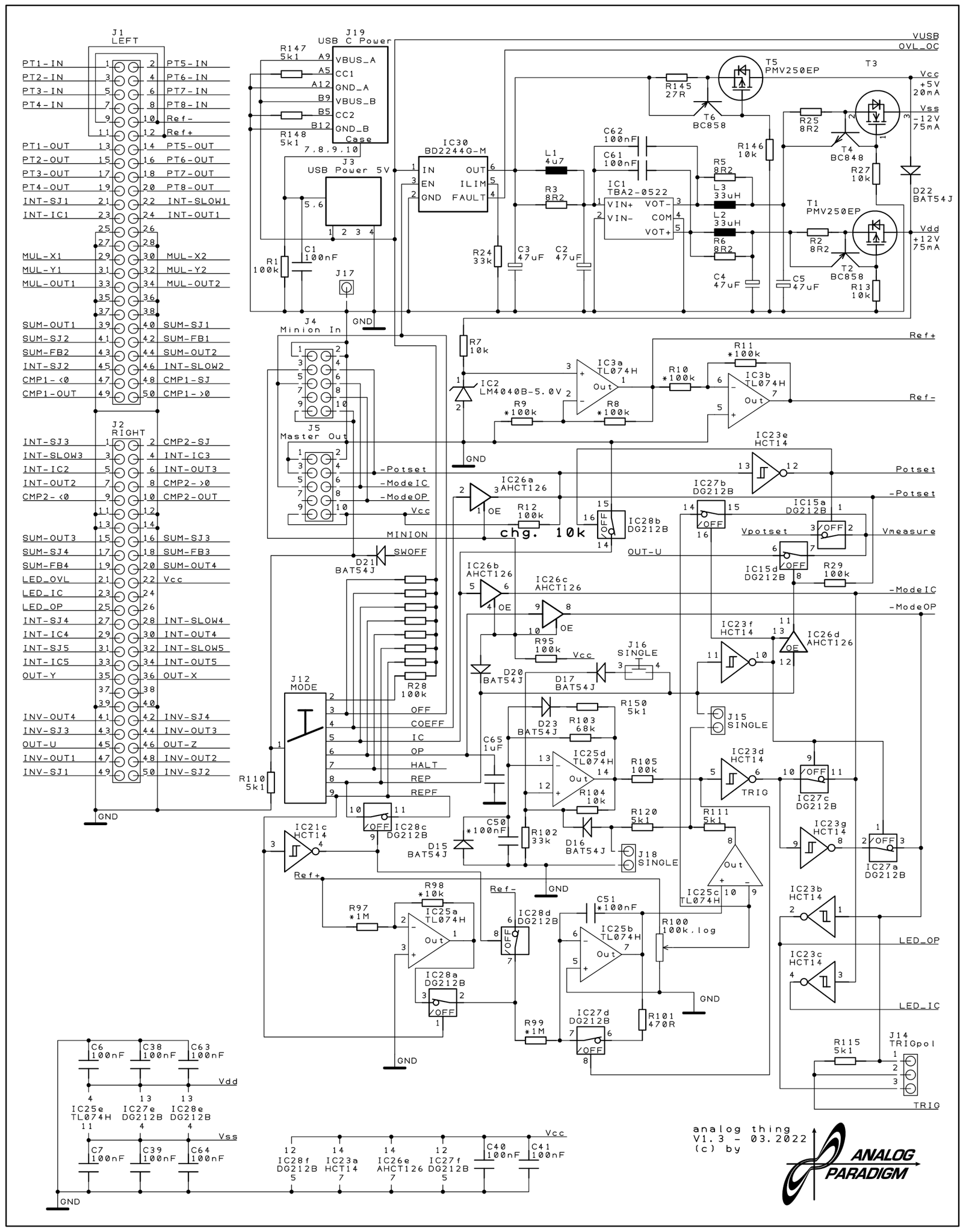
Sheet 01 is the top-level overview sheet. It contains:
Power entry (upper right): The USB-C jack feeds VUSB through a Schottky-protected input to the DC/DC converter block. The converter’s ±12 V outputs (labeled Vdd and Vss) distribute to all functional sub-blocks. Protection zeners clamp transients.
Panel meter (upper center): A 7-segment LCD display module driven by BZX845V zener-referenced circuitry. The input is a buffered, selected voltage from either the coefficient multiplexer chain or the U output jack, depending on mode.
Coefficient potentiometer interface (center left): Eight potentiometer input/output connections route from front-panel connector pads (PTx-IN, PTx-OUT) through the mode-logic multiplexer to the panel-meter input. The coefficient selector knob drives the multiplexer address.
Patch connector map (left column): A dense block of connector pads lists every labeled node — INT-BLKn, INT-ICn, INT-Outn, SUM-Bn, SUM-Fn, INV-Outn, MUL-n, CMP-n, PTx, LEDs, VAx — matching the front-board jack grid. This sheet thus functions as the interface specification between the two PCBs.
Minion control (upper right): The MINION IN / MASTER OUT ports and their direction-control logic appear here, including the 74LVC245S buffer and mode-selector lines (MINION, SNOFF, ModeOP, ModeIC).
2.6.2 Sheet 02 — Coefficient potentiometers, PT buffers, and panel reference
Sheet 02 focuses on the analog signal conditioning between the coefficient potentiometers and the rest of the computing fabric.
PT buffer amplifiers (center): Eight TL074H op-amp sections (IC5b through IC10d in the schematic, four quad packages) buffer the wiper outputs of PT1–PT8. Each buffer is configured as a unity-gain voltage follower. Output resistors (100 Ω, labeled as R16–R23 or similar series) limit current and protect against accidental short circuits at the patch jacks (PT1-OUT through PT8-OUT).
Panel meter reference (upper): Resistors R144 and the TL074H buffer (IC2c) generate the stable ±1 MU reference from the ±12 V rails. The zener D16 (BZX845V) sets an intermediate voltage node labeled Vref. The zener Vmeasure line (R9a, 15 kΩ reference resistor visible at upper right) feeds the meter.
Decoupling array (bottom): Pairs of 100 nF capacitors (ICs C10–C25 range) at each op-amp VDD/VSS pin are drawn as a compact grid. All capacitors bypass at the supply pins of every TL074H package on this sheet.
2.6.3 Sheet 03 — Integrators, summers, and inverters
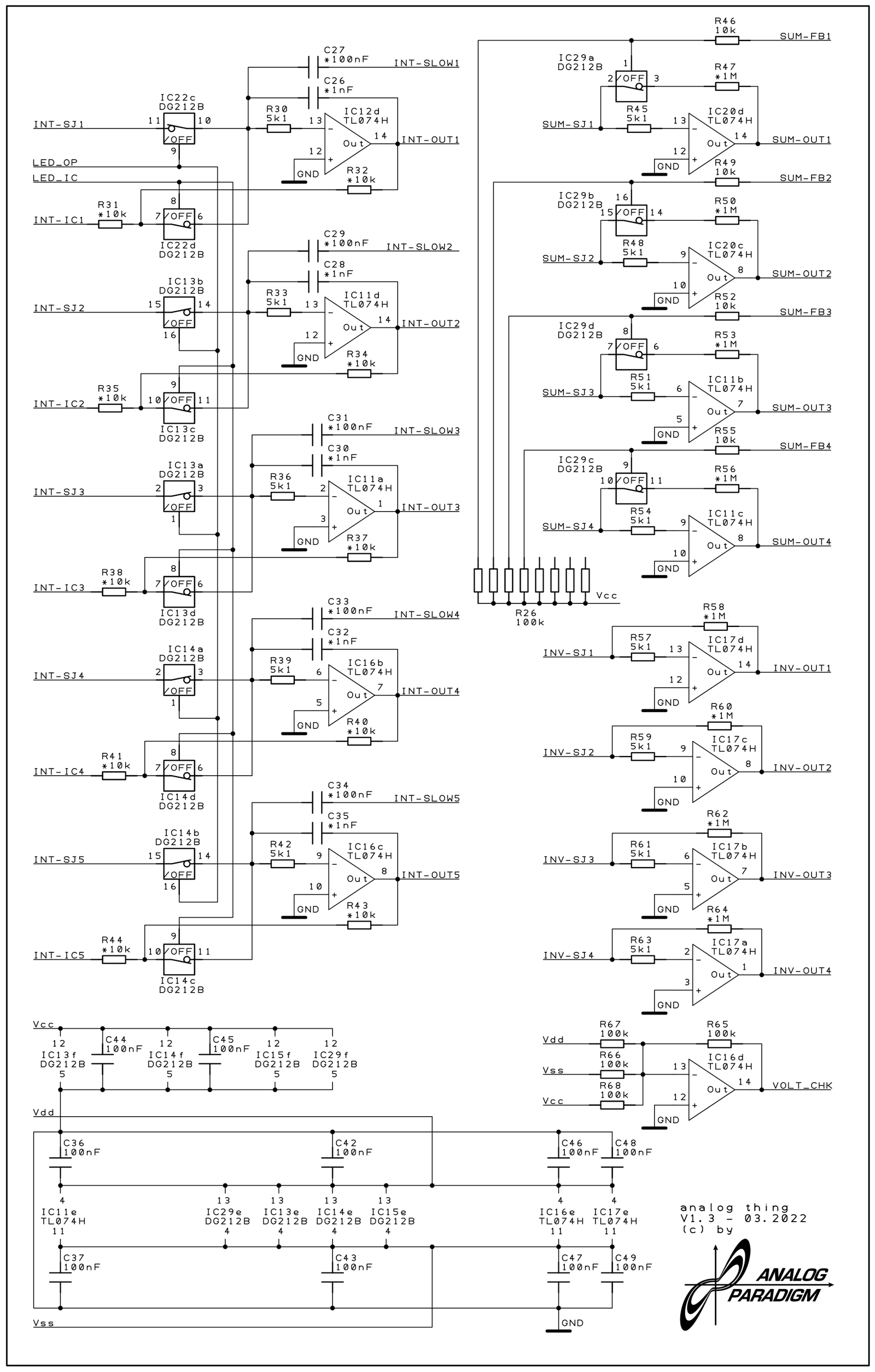
Sheet 03 is the computational heart of the base board, containing all linear computing elements.
Integrators INT1–INT5 (left column): Five DD212B analog switch packages control IC/OP switching at each integrator. Each integrator cell shows: a DD212B switch array gated by the IC/OP control line, a weighted resistor network (five resistors per integrator, with two at R/10 for ×10 weighting), a feedback capacitor C (labeled C24–C28 or similar), and a TL074H section as the Miller integrator op-amp. The front-panel schematic (front sheet 02) clearly labels INT1 through INT5; this count of five integrators is confirmed by the First Steps manual and the front-panel schematics.
Summers SUM1–SUM4 (right column, upper): Four summer cells each use a TL074H section with seven input resistors. Three R/10 resistors provide ×10 weighted inputs; four R resistors provide unity inputs. The SUM-B (inverting output) and SUM-F (feedback-point) jacks connect to the front panel via the connector map from sheet 01.
Inverters INV1/2 and INV3/4 (right column, lower): Two groups of inverting unity-gain amplifiers, each pair sharing a single TL074H quad package. Each inverter cell has one input and two output jacks (INV-Out). A separate unity-gain stage provides the VOLT-CHK signal for the overload LED detection chain (OL LED, visible bottom right).
Overload detection (bottom right): A LM6392-type comparator (or equivalent, visible as IC in the bottom right area of sheet 04) monitors output excursion beyond the machine unit boundaries. If any output exceeds approximately ±10 V, the OL (overload) LED on the front panel illuminates.
2.6.4 Sheet 04 — Multipliers, comparators, and LED drive
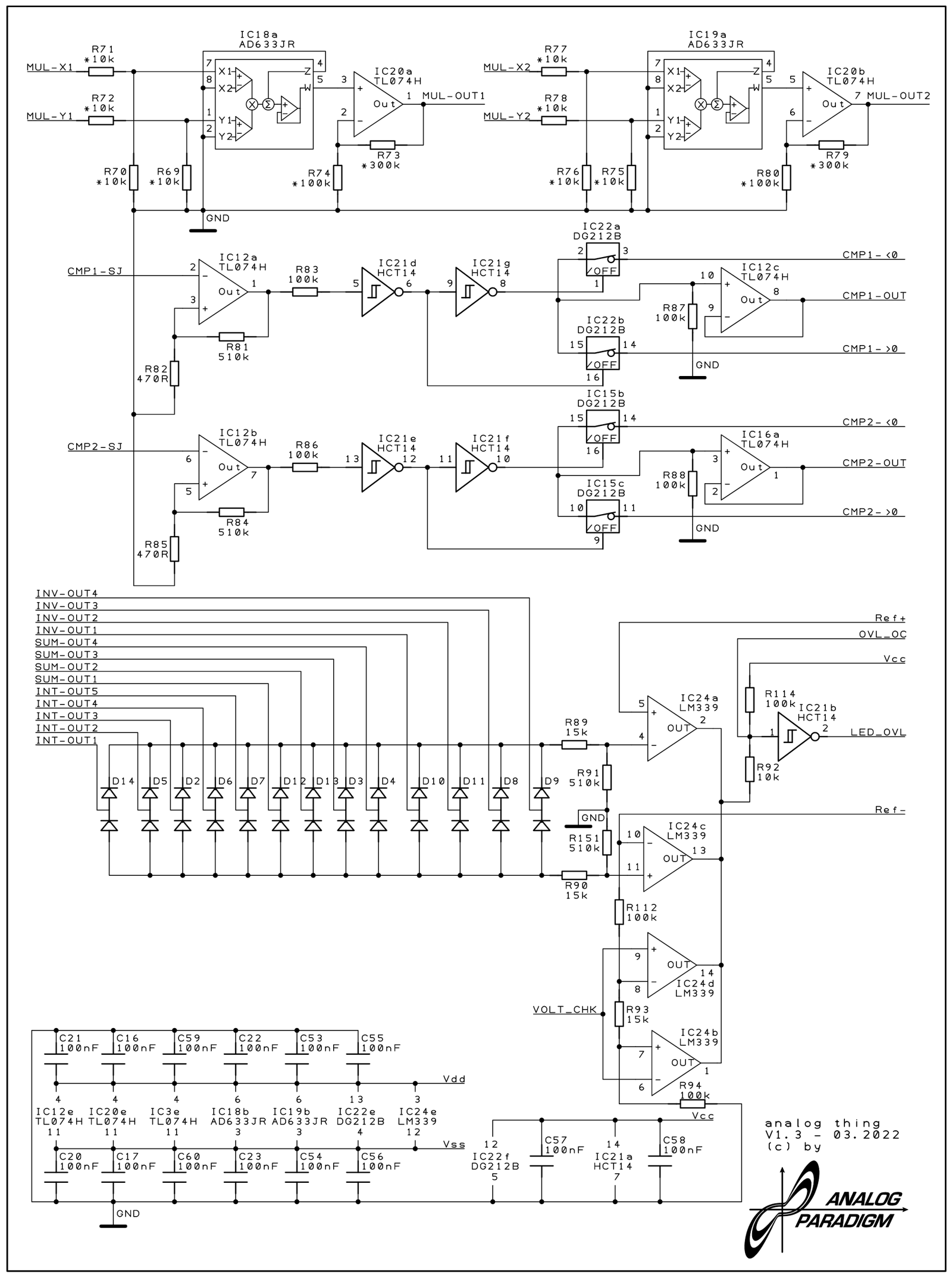
Multipliers MUL1, MUL2 (upper left): Each multiplier uses a four-quadrant analog multiplier IC (consistent with AD633 or equivalent; the IC designator at available image resolution shows a DIP-8 outline). Input resistors R7x (100 Ω series, four per multiplier) protect the multiplier inputs from patch-cable shorts. The output is routed to MUL-OUT jacks on the front panel. The two multipliers are independent; no cross-connection is present in the schematic.
Comparators CMP1, CMP2 (center): Each comparator cell consists of two TL074H sections and a switching network: a high-gain first stage provides the sign decision, and the second stage implements the analog mux function (route > input or < input to output). The switching uses DD212B analog switches gated by the comparator decision output. Output jacks CMP1-OUT and CMP2-OUT (two each) appear on the front panel.
LED drive (center-right): Multiple TL074H sections drive LEDs (labeled LED-OP, LED-IC, LED-OL in the schematic) through resistors R (316 Ω typical), producing the three front-panel state indicators: OP (green, patch running), IC (yellow, initial condition), OL (red, overload).
Overload detection (lower right): A dedicated op-amp comparator stage (VOLT-CHK net from sheet 03) monitors a summed sample of all outputs via a diode network. When any signal exceeds the threshold, it drives the OL LED and potentially the comparator outputs for user feedback.
Decoupling (bottom): The lower strip of sheet 04 shows additional 100 nF bypass capacitors (IC54a–IC56 series) for the multiplier and comparator supply rails.
2.6.5 Sheet 05 — Back-panel I/O, HYBRID port, TRIG output, and RCA attenuation
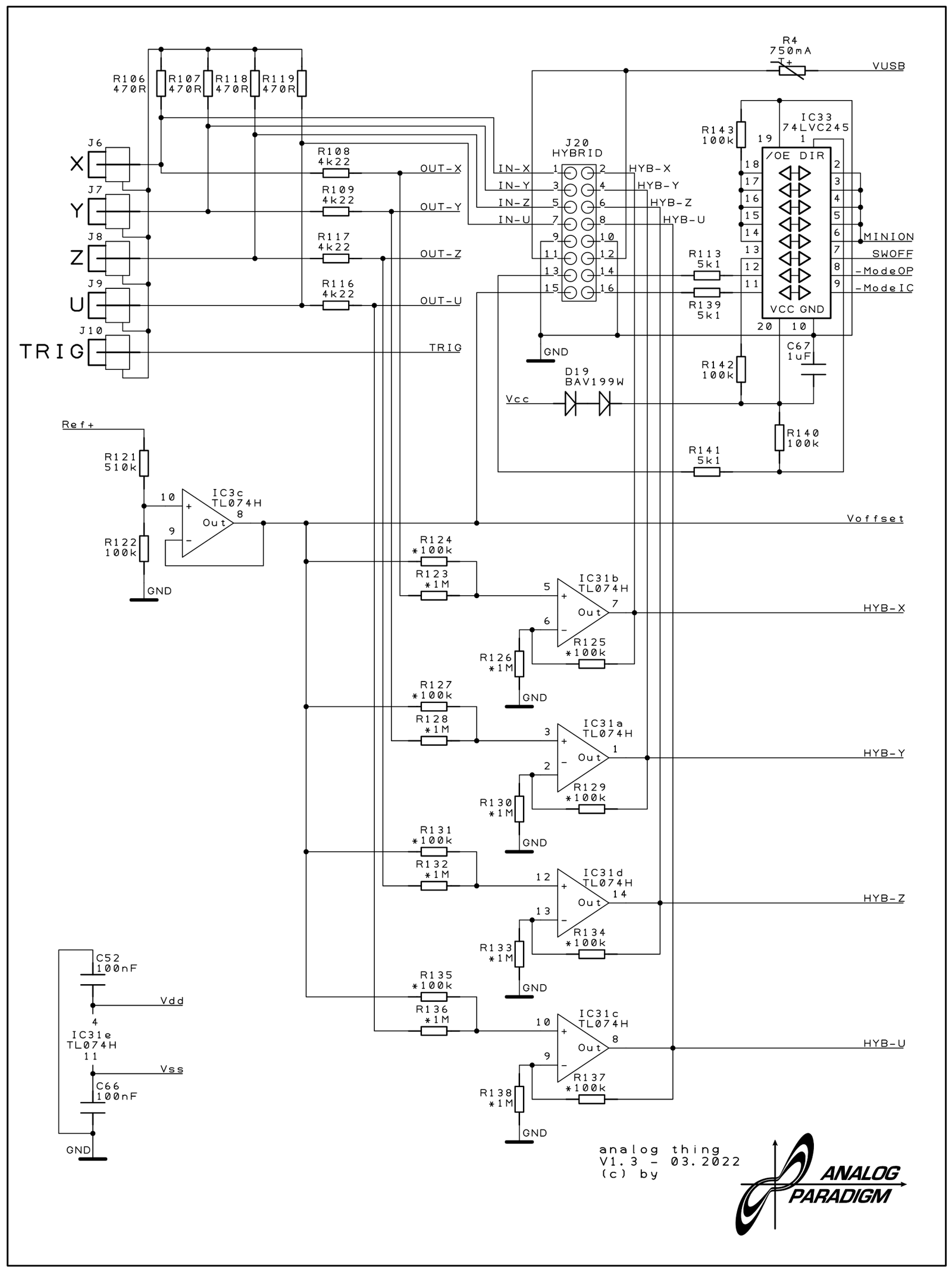
Sheet 05 documents all signals leaving or entering the board at the rear panel.
RCA output attenuation (upper left): Four attenuation chains, one for X, Y, Z, and U outputs. Each chain uses two resistors (R116/117/118/119, all labeled 470 Ω) forming a voltage divider that reduces ±10 V to approximately ±1 V for the RCA jacks. The TRIG signal (R16, 71 Ω) drives the RCA TRIG OUT jack with a logic-level trigger pulse in REP/REPF modes.
Reference buffer (left center): A TL074H section (IC2c/IC2e visible as “18, 9, Out” in schematic) provides the Voffset1 reference used across the output attenuation network.
HYBRID port (center): The 32J HYBRID connector routes the four output signals through the IC31a–d quad TL074H stage. Each section adds a DC offset and scales the ±10 V machine unit to 0–3.3 V (nominally: offset = +1 MU, gain = 3.3/20). Resistors R123–R137 (all 100 Ω or 1 kΩ, values partially confirmed at available resolution) set the scaling. The resulting HYB-X, HYB-Y, HYB-Z, HYB-U signals appear at the HYBRID connector alongside VCC, GND, and digital mode-control lines.
Minion/master interface (upper right): The 74LVC245S octal buffer (IC33) drives the MINION OUT ribbon connector. Its direction pin is controlled by the mode-selector: in MASTER mode the buffer drives outward; in MINION mode it receives. The IC33 operates at 3.3 V (VCC), level-shifting between the logic bus and the 5 V ribbon cable. A 100 kΩ pull-down (R140) holds the bus quiescent. A 1 µF capacitor (C67) decouples VCC at the buffer.
2.7 Schematic walk — front board sheets 01–02
2.7.1 Sheet 01 — Jack field layout, coefficient pot wiring, multiplier/comparator fronts, and XIR networks
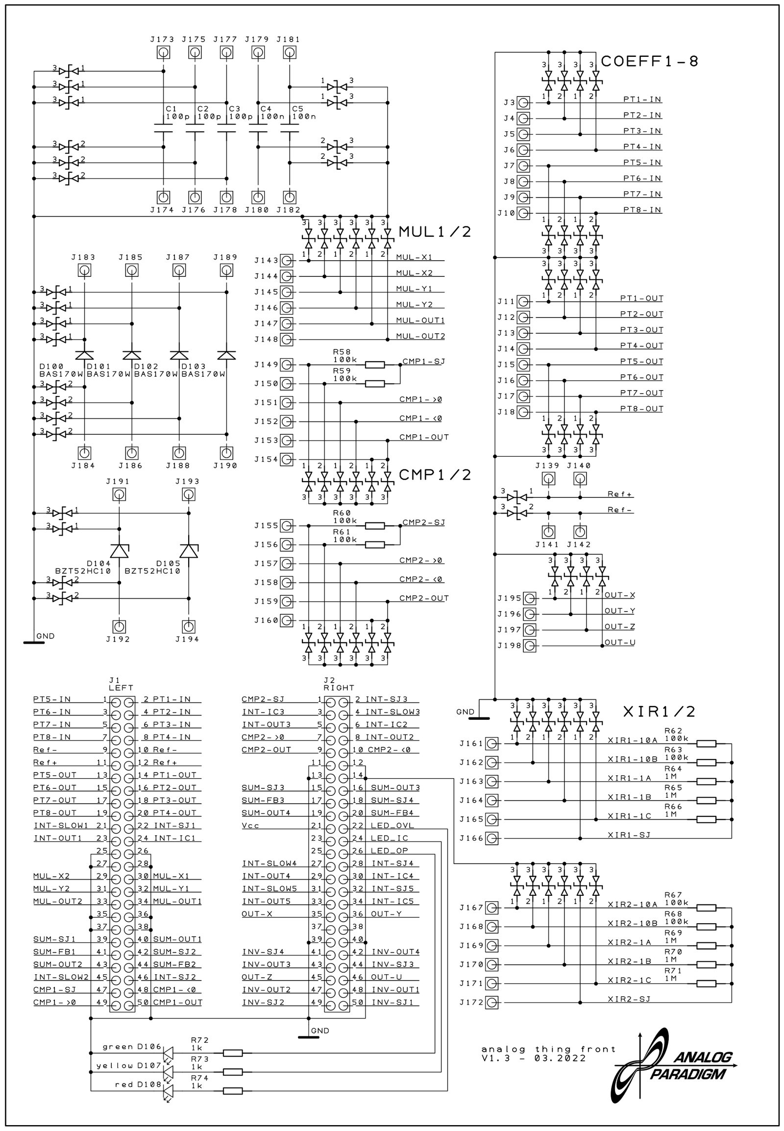
Front-board sheet 01 is essentially the connector-to-connector wiring diagram for the patch panel PCB. Key observations:
Coefficient section (upper left): COEFF1–8 (labeled as a grouped block) shows the input and output connector pads for PT1–PT8, connected to the back-plane connector to the base board.
Multiplier front jacks (MUL1/2, center): The MUL1 and MUL2 jack groups each show: two input jack pads (X and Y inputs), one output jack pad, and additional pads for the output second copy. The jack designators visible in the schematic are 71xx series.
Comparator front jacks (CMP1/2, center-right): The CMP1 and CMP2 groups show A-input, B-input, and two output jack pads per comparator, plus the switching-input jacks (> and <).
XIR resistor networks (lower right): Two XIR blocks (XIR1, XIR2) each present a summing junction (SJ jack), a bank of input jacks, and the common output to the SJ of the connected computing element. These allow adding more inputs to an integrator or summer beyond its built-in count by bridging the XIR SJ to the element SJ jack.
Full patch field connector matrix (left column): A large block of 71xx series connector pads maps every labeled node on the front panel to the corresponding base-board through-connector. The patch panel PCB through-holes double as both the jack field (accessible to the operator) and the inter-board interface.
2.7.2 Sheet 02 — INT1–5, SUM1–4, INV1/2, INV3/4 front-panel connector detail
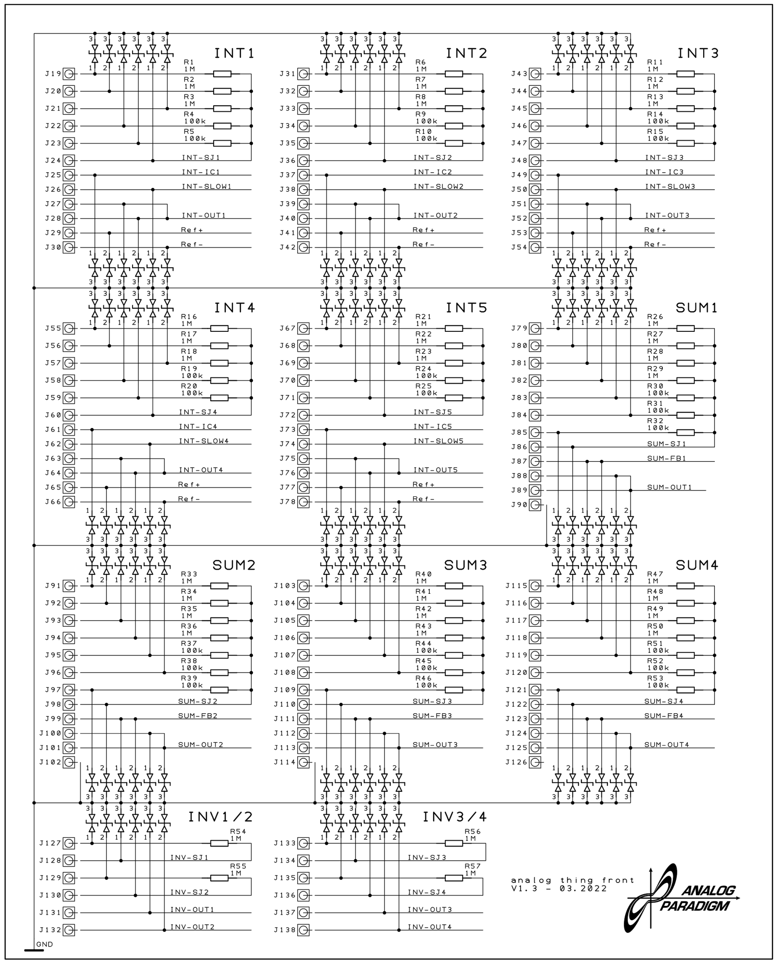
Front-board sheet 02 provides the granular connector-pad layout for each linear computing element as it appears on the top surface of the front PCB.
Integrators INT1–INT5 (upper two rows): Each integrator block shows the same repeating template of connector pads:
- Five input pads (three ×1, two ×10)
- One IC (initial condition) input pad
- Two output pads (INT-Out and INT-Slow, the dedicated output pair)
- One SJ pad (summing junction, for XIR extension)
The pad designators are in the 71xx and 73xx numeric series. All five integrator blocks (INT1–INT5) are visible on this front-board sheet and are user-accessible. The five integrators count is the authoritative figure confirmed by both the schematic and the First Steps manual.
Summers SUM1–SUM4 (middle rows): Each summer block shows seven input pads and two output pads (SUM-Bn, SUM-Fn for the two output jacks), plus an SJ pad.
Inverters INV1/2, INV3/4 (lower rows): Two groups of two inverter channels each. Each channel has one input pad and two output pads (INV-Out). The INV1/2 group shares one connector block; INV3/4 shares another. This confirms the schematic-based reading of four total inverter channels grouped as two pairs.
Passive-element arrays (not shown in sheet 02): The capacitor array, diode array, and Zener diodes accessible on the front panel are wired through the front-board PCB copper but are mounted as through-hole or SMD components on the front-board surface. Their connector pads appear as auxiliary pad clusters alongside the computing-element groups.
2.8 Summary specification tables
2.8.1 THAT v1.3 hardware specification summary
Table 6 — THAT v1.3 hardware specification summary
| Parameter | Value | Source |
|---|---|---|
| Machine unit voltage range | ±10 V | First Steps manual §5 |
| Op-amp supply rails | ±12 V | FAQ §11; sheet 02 Vdd/Vss labels |
| Power input | 4.5–5.5 V USB-C | First Steps manual §2, §11 |
| DC/DC converter type | Isolated boost, 5 V → ±12 V | FAQ §11; sheet 01 |
| Number of integrators | 5 | First Steps manual §7; front-panel schematic INT1–INT5 |
| Integrator inputs (per element) | 5 (3×unity + 2×ten) + IC | First Steps manual §7 item 7 |
| Number of summers | 4 | First Steps manual §7 item 22 |
| Summer inputs (per element) | 7 (4×unity + 3×ten) | First Steps manual §7 item 22 |
| Number of inverters | 2 pairs (4 channels) | Schematic sheet 03 |
| Number of multipliers | 2 | First Steps manual §7 item 20 |
| Number of comparators | 2 | First Steps manual §7 item 21 |
| Number of coefficient pots | 8 | First Steps manual §7 items 16, 17, 23 |
| Coefficient pot range | 0 to +1 MU (unipolar) | First Steps manual §5 |
| Total patch jacks | 186 | First Steps manual FAQ §11 |
| Patch cable type | 2 mm banana plug | First Steps manual §2, §3 |
| Output jacks (panel) | 4 (X, Y, Z, U) | First Steps manual §7 items 3, 11 |
| RCA output level | ±1 V (attenuated from ±10 V) | First Steps manual §7 item 3 |
| HYBRID port output | 0–3.3 V (shifted + scaled) | First Steps manual §7 item 5 |
| Precision (typical) | ~2 decimal places rel. to MU | First Steps manual FAQ §11 |
| Primary op-amp | TL074H (JFET quad) | Schematics sheets 02–05 |
| Mode selector positions | COEFF, IC, OP, HALT, REP, REPF, MINION | First Steps manual §7 item 14 |
| REP mode OP-time range | 0–10 s | First Steps manual §7 item 15 |
| REPF mode OP-time range | 0–100 ms | First Steps manual §7 item 15 |
| Minion chain limit | Unlimited (per manual) | First Steps manual §7 item 2 |
2.8.2 Computing-element input weights
Table 7 — Computing-element input weights
| Element | ×1 inputs | ×10 inputs | IC input | Sign |
|---|---|---|---|---|
| Integrator | 3 | 2 | 1 | Inverting |
| Summer | 4 | 3 | — | Inverting |
| Inverter | 1 | — | — | Inverting |
| Multiplier | 2 (X, Y) | — | — | Non-inverting (÷10) |
| Comparator | 2 (A+B decision) | — | — | Routing (see text) |
2.8.3 Back-panel connector summary
Table 8 — Back-panel connector summary
| Connector | Signal | Level | Direction |
|---|---|---|---|
| USB-C IN | Power | 4.5–5.5 V DC | In |
| RCA X, Y, Z, U | Analog output | ±1 V | Out |
| RCA TRIG OUT | Trigger pulse | Logic level | Out |
| HYBRID port | HYB-X/Y/Z/U + mode | 0–3.3 V | Bidirectional |
| MASTER OUT | Minion bus | 3.3 V logic ribbon | Out (master) |
| MINION IN | Minion bus | 3.3 V logic ribbon | In (minion) |
2.8.4 Mode selector behavior
Table 9 — Mode selector behavior
| Mode | Integrators | Panel meter shows | TRIG out |
|---|---|---|---|
| COEFF | Held (IC or last OP) | Selected coefficient value (0–1) | Off |
| IC | Loading IC values | U output (±1 range) | Off |
| OP | Integrating | U output (±1 range) | Off |
| HALT | Held at last OP value | U output (±1 range) | Off |
| REP | IC → OP, cycling | OP time (0–10 s) | Pulses each cycle |
| REPF | IC → OP, fast cycling | OP time (0–100 ms) | Pulses each cycle |
| MINION | Controlled by master | U output (±1 range) | Follows master |
2.8.5 Schematic sheet index
Table 10 — Schematic sheet index
| Sheet | Board | Primary content |
|---|---|---|
| Base sheet 01 | Base | Power entry, DC/DC, patch-connector map, coeff MUX, minion logic, panel meter |
| Base sheet 02 | Base | Coefficient pot buffers (TL074H ×8), reference divider, decoupling array |
| Base sheet 03 | Base | Integrators ×5, summers ×4, inverters ×2 pairs (4 total), OL LED detection |
| Base sheet 04 | Base | Multipliers ×2, comparators ×2, LED drivers (OP/IC/OL), overload monitor |
| Base sheet 05 | Base | RCA attenuation, TRIG output, HYBRID port scaling, minion/master buffer |
| Front sheet 01 | Front | Coeff section, MUL/CMP front jacks, XIR networks, full jack pad matrix |
| Front sheet 02 | Front | INT1–5 jack detail, SUM1–4 jack detail, INV1/2 and INV3/4 jack detail |
2.9 Perspective photograph
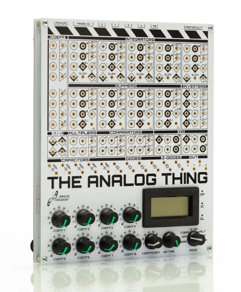
The photograph shows the characteristic layout of THAT’s front panel. The dense 2 mm banana-jack field occupies the upper two-thirds of the panel, with computing element groups separated by labeled silk-screened zones. The eight coefficient potentiometer knobs are arranged in a row in the lower portion of the panel. The panel meter occupies the lower left, flanked by the mode selector rotary switch, the coefficient selector, and the OP-time potentiometer. Three state LEDs (OP/IC/OL) are visible near the meter.
2.10 Architectural design choices — engineering commentary
The following observations are based on direct reading of the schematics and manual, placed in context for an engineer familiar with classical analog computing practice.
TL074H throughout. Using a single quad op-amp type across all linear elements simplifies procurement, reduces component count variants, and ensures consistent slew rate and offset characteristics across integrators, summers, inverters, and the support circuitry. The JFET input stage is essential for the integrator role: input bias current of a bipolar op-amp would produce a systematic integrator drift proportional to I_B × R_f, measurable in seconds-long integrations at the ±10 V machine unit.
DD212B analog switches for IC/OP control. Classic relay-based IC/OP switching (as in PACE TR-48, EAI 580, Telefunken RA 800 era machines) is replaced here with CMOS analog switches. This enables the sub-millisecond switching times required by REPF mode (100 ms total cycle time with multiple IC/OP transitions) while eliminating the mechanical wear, contact bounce, and acoustic noise of relays.
Two-board architecture. Separating the computing circuitry (base board) from the jack field (front board) allows the front-board to be the operator interface — replaceable, cleanable, and manufacturable with through-hole gold-plated 2 mm holes rather than socketed connectors. The base board carries no operator-accessible parts except the rear-panel connectors and the USB-C jack.
Fixed ±10 V machine unit. Classical machines often allowed adjustable machine units or operated at ±100 V. The ±10 V choice places THAT within the safe operating area of modern precision op-amps running on ±12 V and within the input range of modern 3.3 V–5 V ADCs after attenuation, enabling the HYBRID port without additional level-shifting complexity.
Coefficient potentiometer range (0 to +1 only). The unipolar range simplifies the pot mechanism (no center-detent required, no ±precision matching) and keeps the panel meter display non-ambiguous (0–1 displayed). The operator achieves negative coefficients by using an inverter stage or by exploiting the implicit inversion in integrators and summers. This is a deliberate pedagogical choice documented in the First Steps manual helper function §10.4 for ±1 range.
Note — Readers wishing to understand the mathematical theory behind these topology choices — why inverting integrators, why summing-junction architecture, how scaling interacts with element gain — should consult Vol 4 (Programming). The hybrid digital interface and its firmware protocol are detailed in Vol 6 (Expansion & hybrid). For multi-unit chaining signal-flow and the master/minion mode-synchronization protocol, also see Vol 6.
Comments (0)