Heathkit ES-400 · Volume 3
Heathkit ES-400 — Volume 3 — Computing elements & patchbay
Operational amplifier theory, integrator mechanics, patch-field topology, and coefficient scaling — bridges Vol 2 (power) and Vol 4 (problem setup)
3.1 About this Volume
This volume dissects the computing core of the Heathkit ES-400 Electronic Analog Computer — the elements the operator touches, patches, and adjusts every time the machine solves a problem. Volume 2 established how the ES-2 amplifier supply delivers regulated ±250 V and how the ES-50 reference supply holds ±100 V; Volume 4 (problem setup and scaling) builds on the circuits described here. The present volume addresses the patchbay jack field, the ES-201 operational amplifier configured as a summer and as an integrator, the front-panel coefficient potentiometers, sign inversion, the comparator/bias-diode subsystem, and concludes with a single worked element example that ties every concept together.
Readers unfamiliar with the physical sub-assembly layout or power distribution should review Vol 2 before proceeding. Readers who wish to set up multi-amplifier programs (harmonic oscillators, projectile motion, spring-mass-damper chains) should continue to Vol 4 after completing this volume.
Note — Throughout this volume “the manual” refers to the Heath Electronic Analog Computer Operational Manual (Heath Company, Benton Harbor, Michigan) supplied with the ES-400. Page citations match the original document pagination.
3.2 The Patch Field (Patchbay)
3.2.1 Physical Characteristics
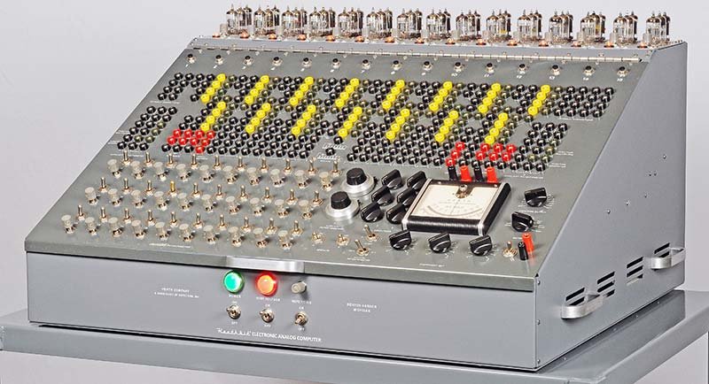
The ES-400 front panel carries 364 banana-plug jacks arranged in a dense grid across the upper two-thirds of the sloped surface. The jacks accept standard 2 mm banana plugs and are spaced at ¾ inch (19 mm) centres both horizontally and vertically, giving the field its distinctive uniform appearance. Every signal path within a programmed setup is realised by inserting a banana-plug patch cord between two or more of these jacks.
The front panel itself is a single heavy-gauge steel sheet, silk-screened in white and grey on a factory-painted satin grey background. It hinges forward on a piano-hinge at the bottom edge, supported during maintenance by locking tip-up rods (the same type used for truck camper shells). When hinged forward, the entire rear wiring harness — soldered to the backs of all 364 jacks — is exposed as a single assembly. The manual and the Goodsell restoration both emphasise that removing the harness as one unit (by unsoldering all jacks from the rear while leaving all wires attached to each other) is the safest disassembly approach, as it preserves the wiring topology for later tracing.
Front-panel zone map (ASCII representation of approximate jack layout):
┌──────────────────────────────────────────────────────────────────────────────┐
│ [AMP 1] [AMP 2] [AMP 3] [AMP 4] [AMP 5] [AMP 6] [AMP 7] [AMP 8] │ ← tubes on top deck
│ [AMP 9] [AMP10] [AMP11] [AMP12] [AMP13] [AMP14] [AMP15] │
├──────────────────────────────────────────────────────────────────────────────┤
│ ●●●●●●●●●●●●●●●●●●●●●●●●●●●●●●●●●●●●●●●●●●●●●●●●●●●●●●●●●●●●●●●●●●●●●●●● │ ← COMPUTING ROWS
│ ●●●●●●●●●●●●●●●●●●●●●●●●●●●●●●●●●●●●●●●●●●●●●●●●●●●●●●●●●●●●●●●●●●●●●●●● │ (amplifier inputs,
│ ●●●●●●●●●●●●●●●●●●●●●●●●●●●●●●●●●●●●●●●●●●●●●●●●●●●●●●●●●●●●●●●●●●●●●●●● │ feedback, outputs)
│ ●●●●●●●●●●●●●●●●●●●●●●●●●●●●●●●●●●●●●●●●●●●●●●●●●●●●●●●●●●●●●●●●●●●●●●●● │
├───────────────────┬──────────────┬───────────────────────────────────────────┤
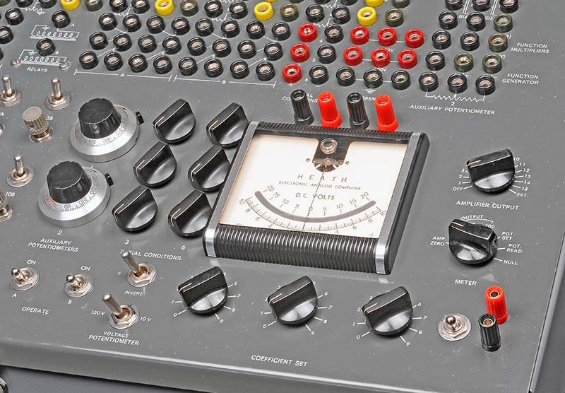
│ RELAYS IC CONDS │ [METER] │ FUNC.GEN AUX POTS BIAS DIODES SCOPE │
│ ● ● ● ● ● ● ● ● │ ┌────────┐ │ ●●●●●● ●●●●●● ●●●●●●●● ●●●● │
│ │ │DC VOLTS│ │ │
│ [OPERATE switches]│ └────────┘ │ [REFERENCE JACKS: +100V, -100V] │
├───────────────────┴──────────────┴───────────────────────────────────────────┤
│ AUX POTS ●● INIT COND ●●●●●● VOLTAGE POTENTIOMETER COEFFICIENT SET │
│ │
│ [COEFF POT 1..30, each with INPUT + WIPER jack pair] │
├──────────────────────────────────────────────────────────────────────────────┤
│ POWER ON ○ HIGH VOLTAGE ON ○ REPETITIVE ON ○ [Heath logo / name] │
└──────────────────────────────────────────────────────────────────────────────┘The upper computing rows contain the highest jack density: each of the 15 amplifier groups has multiple input jacks (the exact count per amplifier depends on the harness wiring — typically five to eight input jacks per amplifier summing junction, reflecting the number of resistor positions available), one feedback jack, and one output jack. Wiring on the back of the panel busses each group to the corresponding ES-201 module connector.
(reference — courtesy Nuts & Volts / David Goodsell)
The jack field is subdivided by function. Looking at the panel from the operator’s perspective:
Table 1 — The jack field is subdivided by function. Looking at the panel from the operator's perspective
| Zone | Location on panel | Function |
|---|---|---|
| Amplifier input/output rows | Upper field, 15 column groups | One column group per ES-201 module — summing junction inputs, feedback jack, amplifier output |
| Reference supply jacks | Right-centre cluster | +100 V and −100 V from the ES-50, brought to panel |
| Initial condition jacks | Left-centre group | Six IC floating supply taps, one pair per ES-100 supply |
| Coefficient pot jacks | Lower-centre row | Input and wiper jacks for each of the 30 standard coefficient pots |
| Auxiliary potentiometer jacks | Lower-right | Input, wiper, and output for the two 10-turn precision pots |
| Bias diode jacks | Right field | Four dual-diode assemblies for nonlinear function generation |
| Relay contacts | Left lower | Normally-open and normally-closed contacts of the two operational relays |
| Oscilloscope output jacks | Centre-lower | Vertical and horizontal outputs for display connection |
| Meter jacks | Centre-right | AMP ZERO / POT READ / NULL positions feed the front-panel DC milliammeter |
| External connection jacks | Rear panel, brought to front | Varicon sockets for the ES-600 function generator and external signals |
3.2.2 Jack Colour and Functional Identification
The manual does not assign mandatory patch-cord colours to signal categories; the operator establishes a personal convention. The recommended convention used in Heath’s own example setups (manual p. 14, Figure 14) employs:
Table 2 — The manual does not assign mandatory patch-cord colours to signal categories; the operator establishes a personal convention. The recommended convention used in Heath's own example setups (manual p. 14, Figure 14) employs
| Colour | Conventional use |
|---|---|
| Black | Electrical ground / common reference |
| Red | High-voltage or “positive-sign” signal paths |
| Yellow | General signal interconnects (amplifier to amplifier) |
| Green | Feedback paths |
| White / other | Coefficient pot connections |
The manual explicitly states that satisfactory operation requires patch cords with low DC resistance and good insulation. For integration, capacitors (and hence amplifier outputs driving integration nodes) are sensitive to leakage. The only satisfactory insulation materials for capacitors used on the ES-400 are polystyrene and polyethylene. Carbon composition and paper capacitors are not acceptable for integration duty (manual p. 14).
3.2.3 The Summing Junction
Each ES-201 module exposes a summing junction (sometimes called the high-gain node) at its input group of jacks. This node is the virtual ground produced by the enormously high open-loop gain (~50,000) of the amplifier driving the junction toward zero volts through negative feedback. Every current injected into this node — by any resistor connected from any input signal — is summed algebraically and appears, inverted and scaled, at the output jack.
  V1 ──[ R1 ]──┐
               │
  V2 ──[ R2 ]──┤── [Σ]──┬──[ Rfb or Cfb ]──→ Output
               │         │
  V3 ──[ R3 ]──┘         │
                          │
                    (Virtual ground
                     = summing junction)
The plug-in resistor and capacitor elements — provided by the operator using the resistor/capacitor set supplied with the ES-400 — physically plug into holes in the jack field directly adjacent to each amplifier’s summing junction and feedback jacks. The resistors and capacitors are 1% tolerance where required.
3.2.4 Signal Range and Loading
All computing signals on the ES-400 operate within the range ±100 V. The ES-201 amplifier output is rated at ±100 V at up to 10 mA continuous. When the output reaches the ±100 V rail, the NE-51 neon overload indicator for that module illuminates (visible on the top deck). An illuminated NE-51 indicates saturation — the computation is invalid at that instant and the problem scaling must be revised (see Vol 4).
The front-panel meter is a DC milliammeter whose deflection indicates voltage. It is switched among three modes by the METER toggle: AMP ZERO (balance adjustment), POT READ (coefficient pot setting), and NULL (used with the AMPLIFIER OUTPUT jack for zero-checking). The meter reads ±20 V full scale across its centre-zero scale.
Note — Loading any amplifier output with more than 10 mA will degrade accuracy. The ES-400’s 364-jack field allows many jacks to be bussed together; if several coefficient pots are driven from a single output, the aggregate load current must remain below 10 mA at full-scale (±100 V) output — implying a minimum combined load resistance of 10 kΩ. In practice, the 1 MΩ input resistors of neighbouring amplifiers pose no problem, but chains of low-value coefficient pot inputs (10 kΩ) can approach this limit.
3.3 The Summer (Inverting Summation Amplifier)
3.3.1 Amplifier Architecture: ES-201
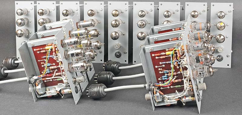
The ES-201 DC Operational Amplifier module is the fundamental computing element. All 15 units in the ES-400 are physically identical modular assemblies that plug into the rear of the front panel via multi-pin connectors. Each module occupies its own sheet-metal enclosure, roughly 3 × 5 × 8 inches, with the three vacuum tubes projecting upward through holes in the top panel of the ES-400 cabinet.
(reference — courtesy Nuts & Volts / David Goodsell)
The ES-201 PCB (phenolic substrate) mounts all passive components — resistors, capacitors, and the NE-51 neon indicator — on one board. The three tube sockets are point-soldered directly to the board. During restoration, Goodsell found that every axial capacitor and carbon composition resistor required replacement; the 1% resistors in the gain-determining positions were typically still within specification, but corrosion on their end caps made replacement prudent.
Simplified ES-201 signal-flow schematic (SVG):
<svg xmlns="http://www.w3.org/2000/svg" viewBox="0 0 680 260" width="680" height="260" font-family="monospace" font-size="12">

  <!-- Title -->
  <text x="10" y="18" fill="#222" font-size="13" font-weight="bold">ES-201 DC Operational Amplifier — Signal Flow (simplified)</text>

  <!-- INPUT RESISTORS / SUMMING JUNCTION -->
  <text x="10" y="50" fill="#555" font-size="11">Input</text>
  <text x="10" y="62" fill="#555" font-size="11">jacks</text>
  <line x1="50" y1="55" x2="100" y2="55" stroke="#333" stroke-width="1.5"/>
  <line x1="50" y1="80" x2="100" y2="80" stroke="#333" stroke-width="1.5"/>
  <line x1="50" y1="105" x2="100" y2="105" stroke="#333" stroke-width="1.5"/>
  <!-- Resistors -->
  <rect x="62" y="47" width="26" height="16" fill="#fff" stroke="#555" stroke-width="1" rx="2"/>
  <text x="63" y="59" fill="#333" font-size="10">R1</text>
  <rect x="62" y="72" width="26" height="16" fill="#fff" stroke="#555" stroke-width="1" rx="2"/>
  <text x="63" y="84" fill="#333" font-size="10">R2</text>
  <rect x="62" y="97" width="26" height="16" fill="#fff" stroke="#555" stroke-width="1" rx="2"/>
  <text x="63" y="109" fill="#333" font-size="10">R3</text>
  <!-- Converge to summing junction -->
  <line x1="100" y1="55" x2="118" y2="80" stroke="#333" stroke-width="1.5"/>
  <line x1="100" y1="80" x2="118" y2="80" stroke="#333" stroke-width="1.5"/>
  <line x1="100" y1="105" x2="118" y2="80" stroke="#333" stroke-width="1.5"/>
  <circle cx="118" cy="80" r="4" fill="#333"/>
  <text x="106" y="74" fill="#888" font-size="10">Σ</text>
  <text x="96" y="122" fill="#888" font-size="9">≈0V (virtual gnd)</text>

  <!-- 12AX7 Stage -->
  <ellipse cx="185" cy="80" rx="38" ry="50" fill="#f0f4ff" stroke="#336" stroke-width="1.5"/>
  <text x="163" y="68" fill="#336" font-size="11" font-weight="bold">12AX7</text>
  <text x="163" y="82" fill="#336" font-size="10">dual triode</text>
  <text x="163" y="94" fill="#336" font-size="10">high-gain</text>
  <text x="163" y="106" fill="#336" font-size="10">input stage</text>
  <line x1="118" y1="80" x2="147" y2="80" stroke="#333" stroke-width="1.5"/>
  <line x1="223" y1="80" x2="255" y2="80" stroke="#333" stroke-width="1.5"/>

  <!-- 6BQ7 Stage -->
  <ellipse cx="305" cy="80" rx="36" ry="50" fill="#f0fff0" stroke="#363" stroke-width="1.5"/>
  <text x="283" y="68" fill="#363" font-size="11" font-weight="bold">6BQ7</text>
  <text x="283" y="82" fill="#363" font-size="10">dual triode</text>
  <text x="283" y="94" fill="#363" font-size="10">intermediate</text>
  <text x="283" y="106" fill="#363" font-size="10">gain stage</text>
  <line x1="255" y1="80" x2="269" y2="80" stroke="#333" stroke-width="1.5"/>
  <line x1="341" y1="80" x2="373" y2="80" stroke="#333" stroke-width="1.5"/>

  <!-- 6BH6 Stage -->
  <ellipse cx="420" cy="80" rx="36" ry="50" fill="#fff8f0" stroke="#663" stroke-width="1.5"/>
  <text x="398" y="68" fill="#663" font-size="11" font-weight="bold">6BH6</text>
  <text x="398" y="82" fill="#663" font-size="10">pentode</text>
  <text x="398" y="94" fill="#663" font-size="10">output</text>
  <text x="398" y="106" fill="#663" font-size="10">driver</text>
  <line x1="373" y1="80" x2="384" y2="80" stroke="#333" stroke-width="1.5"/>

  <!-- Output -->
  <line x1="456" y1="80" x2="530" y2="80" stroke="#333" stroke-width="1.5"/>
  <text x="535" y="78" fill="#222" font-size="12" font-weight="bold">OUTPUT</text>
  <text x="535" y="92" fill="#555" font-size="11">±100V @ 10mA</text>
  <circle cx="520" cy="80" r="4" fill="#333"/>

  <!-- Feedback path -->
  <line x1="520" y1="80" x2="520" y2="185" stroke="#c33" stroke-width="1.5" stroke-dasharray="5,3"/>
  <line x1="520" y1="185" x2="118" y2="185" stroke="#c33" stroke-width="1.5" stroke-dasharray="5,3"/>
  <line x1="118" y1="185" x2="118" y2="80" stroke="#c33" stroke-width="1.5" stroke-dasharray="5,3"/>
  <!-- Feedback element label -->
  <rect x="270" y="175" width="110" height="20" fill="#fff3f3" stroke="#c33" stroke-width="1" rx="3"/>
  <text x="274" y="189" fill="#c33" font-size="11">Rfb (summer) or Cfb (integrator)</text>
  <text x="280" y="210" fill="#c33" font-size="10">← plug-in component at feedback jack →</text>
  <text x="10" y="215" fill="#c33" font-size="10" font-style="italic">Feedback path (red dashed)</text>

  <!-- NE-51 -->
  <circle cx="530" cy="140" r="12" fill="#ffff99" stroke="#aa8800" stroke-width="1.5"/>
  <text x="520" y="145" fill="#665500" font-size="10">NE-51</text>
  <line x1="520" y1="80" x2="530" y2="128" stroke="#aa8800" stroke-width="1" stroke-dasharray="3,2"/>
  <text x="545" y="145" fill="#665500" font-size="10">overload indicator</text>
  <text x="545" y="157" fill="#665500" font-size="10">(lights at ±100V)</text>

  <!-- Open-loop gain annotation -->
  <text x="185" y="170" fill="#336" font-size="11" font-style="italic">Total open-loop gain ≈ 50,000 (94 dB)</text>
</svg>
(reference — courtesy Nuts & Volts / David Goodsell)
Tube complement per ES-201 module:
Table 3 — Tube complement per ES-201 module:
| Stage | Tube type | Function |
|---|---|---|
| 1st (input) | 12AX7 | Dual triode; high-gain differential input stage; very high input impedance |
| 2nd (intermediate) | 6BQ7 | Dual triode; TV-tuner type; intermediate gain and phase correction |
| 3rd (output) | 6BH6 | Sharp-cutoff pentode; output driver / buffer, provides output current |
| Indicator | NE-51 | Neon lamp; overload / saturation indicator |
The cascade of three stages produces an open-loop voltage gain of approximately 50,000 (94 dB). This very high gain makes the amplifier behave as an ideal op-amp when negative feedback is applied: the summing junction is held to within microvolts of zero, and the closed-loop behaviour is determined almost entirely by the external feedback network.
ES-201 electrical parameters (from manual and Research Guide):
Table 4 — ES-201 electrical parameters (from manual and Research Guide):
| Parameter | Value |
|---|---|
| Open-loop DC gain | ~50,000 |
| Input voltage range | ±100 V |
| Output voltage range | ±100 V |
| Output current (continuous) | 10 mA max |
| Equivalent input noise | Not specified in available sources |
| Input impedance (summing junction) | Determined by external resistors |
| Supply rails | +250 V, −250 V, −450 V from ES-2; +100 V, −100 V from ES-50 |
| Balance adjustment | Front-panel trimmer per module (labelled 1–15) |
3.3.2 Summation Circuit Theory
When resistors are placed at the input jacks and a resistor is placed at the feedback jack, the ES-201 operates as an inverting weighted summer. The closed-loop transfer function for N inputs is:
              Rfb        Rfb        Rfb
Eout = − ( ――――― E1 + ――――― E2 + ――――― E3 + … )
              R1         R2         R3
where R1, R2, R3 are the individual input resistors and Rfb is the single feedback resistor. All resistors are in megohms in the ES-400’s standard resistor set.
Standard resistor set and resulting gains:
Table 5 — Standard resistor set and resulting gains:
| Input resistor (MΩ) | Feedback resistor (MΩ) | Closed-loop gain magnitude |
|---|---|---|
| 1 | 1 | 1 (unity inverter) |
| 1 | 10 | 10 |
| 0.1 | 1 | 10 |
| 1 | 0.1 | 0.1 |
| 0.5 | 1 | 2 |
| 1 | 0.5 | 0.5 |
Note — The ES-400 resistor and capacitor set contains values suited to the machine’s ±100 V signal range. The manual specifies that resistors should be 1% metal film (or equivalent) for accurate summation. Carbon composition resistors with their ±5–10% tolerance and thermal drift are not adequate for precision computing, particularly for scale factors that must hold over a problem run.
3.3.3 The Single-Ended Inverter
The simplest configuration of the summer is a single input with equal input and feedback resistors. The output is then exactly the negative of the input:
Ein ──[ 1MΩ ]──[Σ]──[ 1MΩ (fb) ]──→ Eout = −EinThis configuration, called a sign inverter or simply an inverter, is used ubiquitously whenever a problem requires a positive copy of a variable that only exists with negative sign (a common artifact of the double-inversion in integrator chains). One ES-201 module consumed as a pure inverter is the “cheapest” computing element on the ES-400.
3.3.4 SVG Block Diagram — Summer
<svg xmlns="http://www.w3.org/2000/svg" viewBox="0 0 520 200" width="520" height="200" font-family="monospace" font-size="13">
  <!-- Input signals -->
  <line x1="10" y1="60" x2="120" y2="60" stroke="#333" stroke-width="1.5"/>
  <line x1="10" y1="100" x2="120" y2="100" stroke="#333" stroke-width="1.5"/>
  <line x1="10" y1="140" x2="120" y2="140" stroke="#333" stroke-width="1.5"/>
  <!-- Resistors (zig-zag style label boxes) -->
  <rect x="45" y="50" width="40" height="20" fill="none" stroke="#555" stroke-width="1.2" rx="2"/>
  <rect x="45" y="90" width="40" height="20" fill="none" stroke="#555" stroke-width="1.2" rx="2"/>
  <rect x="45" y="130" width="40" height="20" fill="none" stroke="#555" stroke-width="1.2" rx="2"/>
  <text x="47" y="64" fill="#333" font-size="11">R1</text>
  <text x="47" y="104" fill="#333" font-size="11">R2</text>
  <text x="47" y="144" fill="#333" font-size="11">R3</text>
  <!-- Input labels -->
  <text x="12" y="56" fill="#555" font-size="11">E1</text>
  <text x="12" y="96" fill="#555" font-size="11">E2</text>
  <text x="12" y="136" fill="#555" font-size="11">E3</text>
  <!-- Summing junction node -->
  <line x1="120" y1="60" x2="140" y2="100" stroke="#333" stroke-width="1.5"/>
  <line x1="120" y1="100" x2="140" y2="100" stroke="#333" stroke-width="1.5"/>
  <line x1="120" y1="140" x2="140" y2="100" stroke="#333" stroke-width="1.5"/>
  <circle cx="140" cy="100" r="4" fill="#555"/>
  <text x="130" y="94" fill="#888" font-size="10">Σ</text>
  <!-- Amplifier triangle -->
  <polygon points="160,70 160,130 230,100" fill="#eef" stroke="#333" stroke-width="1.5"/>
  <text x="176" y="104" fill="#333" font-size="12">A≈50k</text>
  <!-- Feedback path -->
  <line x1="230" y1="100" x2="270" y2="100" stroke="#333" stroke-width="1.5"/>
  <line x1="270" y1="100" x2="270" y2="50" stroke="#333" stroke-width="1.5"/>
  <line x1="270" y1="50" x2="140" y2="50" stroke="#333" stroke-width="1.5"/>
  <line x1="140" y1="50" x2="140" y2="100" stroke="#333" stroke-width="1.5"/>
  <rect x="183" y="40" width="48" height="20" fill="none" stroke="#555" stroke-width="1.2" rx="2"/>
  <text x="186" y="54" fill="#333" font-size="11">Rfb</text>
  <!-- Output -->
  <line x1="270" y1="100" x2="340" y2="100" stroke="#333" stroke-width="1.5"/>
  <text x="345" y="88" fill="#333" font-size="12">Eout =</text>
  <text x="345" y="104" fill="#333" font-size="11">−(Rfb/R1·E1</text>
  <text x="345" y="118" fill="#333" font-size="11"> +Rfb/R2·E2</text>
  <text x="345" y="132" fill="#333" font-size="11"> +Rfb/R3·E3)</text>
  <!-- Virtual ground label -->
  <text x="110" y="165" fill="#888" font-size="10" font-style="italic">summing junction ≈ 0 V (virtual gnd)</text>
</svg>
3.3.5 Amplifier Balancing Procedure
Before solving any problem, each ES-201 module must be balanced (nulled). The high DC gain means even small input offset voltages are amplified to large errors at the output. The manual specifies the following procedure (p. 13):
- Place the METER switch to AMP ZERO.
- Confirm no patch cords are connected to the amplifier’s summing junction jacks.
- Connect the amplifier’s OUTPUT jack to the panel meter via the AMPLIFIER OUTPUT jack.
- Adjust the front-panel BALANCE trimmer (numbered 1–15, one per amplifier) until the meter reads zero.
- Install all intended input and feedback components and re-check balance; re-adjust if drift exceeds acceptable limits.
The balance procedure should be repeated after the machine has been powered for at least 30 minutes, allowing all tubes to reach thermal equilibrium. The 12AX7 input stage is particularly sensitive to cathode temperature; the open-loop gain of 50,000 magnifies any cathode-heater leakage or grid-emission offset into a measurable DC error.
3.4 The Integrator
3.4.1 Principle of Integration
Replacing the feedback resistor with a feedback capacitor transforms the ES-201 summer into an integrator. With a capacitor C in the feedback path and a resistor R at the input, the output voltage at time t is:
            1
Eout(t) = − ――― ∫[0→t]  Ein(τ) dτ + Eout(0)
            RC
where Eout(0) is the initial condition (IC) voltage. The quantity 1/RC is the integration rate constant (units: s⁻¹). The minus sign represents the inversion inherent in the amplifier.
3.4.2 Circuit Configuration
  Ein ──[ R ]──[Σ]──┬──[ C (feedback) ]──→ Eout
                    │
                   (Virtual ground)
                    │
                   [Summing junction → held ≈ 0 V by feedback]
Standard time constants using the ES-400 resistor/capacitor set:
Table 6 — Standard time constants using the ES-400 resistor/capacitor set:
| Input resistor R | Feedback capacitor C | Time constant RC | Integration rate 1/RC |
|---|---|---|---|
| 1 MΩ | 1 µF | 1 s | 1 V/V·s |
| 1 MΩ | 0.1 µF | 0.1 s | 10 V/V·s |
| 0.1 MΩ | 1 µF | 0.1 s | 10 V/V·s |
| 1 MΩ | 10 µF | 10 s | 0.1 V/V·s |
| 0.5 MΩ | 1 µF | 0.5 s | 2 V/V·s |
The 1 MΩ / 1 µF combination (RC = 1 s) is the most common setup and the one used in the manual’s worked examples. A constant input of −100 V will ramp the output at +100 V/s, reaching full scale in exactly one second.
Note — The manual (p. 15) cautions that the peak output voltage must not be allowed to exceed ±100 V under normal operating conditions. For a typical problem run time of 1 s with a 1 MΩ / 1 µF integrator, the average input must remain below ±100 V to prevent saturation. Amplitude scaling (Vol 4) ensures this constraint is respected at problem setup time.
3.4.3 Integrator SVG Block Diagram
<svg xmlns="http://www.w3.org/2000/svg" viewBox="0 0 560 190" width="560" height="190" font-family="monospace" font-size="12">

  <!-- Title -->
  <text x="10" y="18" fill="#222" font-size="13" font-weight="bold">ES-201 Configured as Integrator (RC = 1 s typical)</text>

  <!-- Input signal -->
  <text x="10" y="58" fill="#555" font-size="11">Ein</text>
  <line x1="38" y1="54" x2="95" y2="54" stroke="#333" stroke-width="1.5"/>

  <!-- Input resistor R -->
  <rect x="55" y="44" width="28" height="18" fill="#fff" stroke="#555" stroke-width="1.2" rx="2"/>
  <text x="57" y="57" fill="#333" font-size="11">1MΩ</text>

  <!-- Summing node -->
  <circle cx="110" cy="54" r="4" fill="#333"/>
  <text x="98" y="72" fill="#888" font-size="9">Σ≈0V</text>

  <!-- Amplifier box -->
  <rect x="125" y="28" width="80" height="52" fill="#eef0ff" stroke="#333" stroke-width="1.5" rx="4"/>
  <text x="130" y="47" fill="#333" font-size="11">ES-201</text>
  <text x="130" y="61" fill="#333" font-size="10">A ≈ 50,000</text>
  <text x="130" y="73" fill="#333" font-size="10">3-stage tube</text>
  <line x1="110" y1="54" x2="125" y2="54" stroke="#333" stroke-width="1.5"/>

  <!-- Output line -->
  <line x1="205" y1="54" x2="290" y2="54" stroke="#333" stroke-width="1.5"/>
  <circle cx="270" cy="54" r="4" fill="#333"/>

  <!-- Output label -->
  <text x="300" y="42" fill="#222" font-size="11" font-weight="bold">Eout(t) =</text>
  <text x="300" y="56" fill="#333" font-size="11">−(1/RC) ∫Ein dt</text>
  <text x="300" y="70" fill="#555" font-size="10">+Eout(0) initial condition</text>
  <text x="300" y="84" fill="#555" font-size="10">RC = 1MΩ × 1µF = 1 s</text>

  <!-- Feedback capacitor path -->
  <line x1="270" y1="54" x2="270" y2="148" stroke="#c33" stroke-width="1.5" stroke-dasharray="4,3"/>
  <line x1="270" y1="148" x2="110" y2="148" stroke="#c33" stroke-width="1.5" stroke-dasharray="4,3"/>
  <line x1="110" y1="148" x2="110" y2="54" stroke="#c33" stroke-width="1.5" stroke-dasharray="4,3"/>

  <!-- Capacitor symbol on feedback path -->
  <line x1="180" y1="142" x2="180" y2="154" stroke="#c33" stroke-width="2"/>
  <line x1="172" y1="142" x2="188" y2="142" stroke="#c33" stroke-width="2"/>
  <line x1="172" y1="154" x2="188" y2="154" stroke="#c33" stroke-width="2"/>
  <text x="192" y="155" fill="#c33" font-size="11">Cfb = 1µF</text>
  <text x="192" y="168" fill="#c33" font-size="10">(polystyrene)</text>

  <!-- IC relay connection -->
  <line x1="270" y1="54" x2="350" y2="54" stroke="#333" stroke-width="1.5"/>
  <rect x="360" y="40" width="90" height="28" fill="#fffbe6" stroke="#a85" stroke-width="1.2" rx="3"/>
  <text x="365" y="52" fill="#a85" font-size="10">IC relay (ES-151)</text>
  <text x="365" y="64" fill="#a85" font-size="10">presets cap to IC value</text>
  <line x1="350" y1="54" x2="360" y2="54" stroke="#a85" stroke-width="1" stroke-dasharray="3,2"/>

  <!-- Mode annotation -->
  <text x="10" y="178" fill="#555" font-size="10" font-style="italic">In IC mode: relay connects IC supply to output, precharging Cfb. In OPERATE: relay opens, integration begins.</text>
</svg>
3.4.4 Capacitor Dielectric Requirements
This requirement is critical. The manual explicitly states (p. 14): “The only satisfactory insulation materials for capacitors which are to be used in this computer are polystyrene and polyethylene.” Paper and electrolytic capacitors have excessive dielectric absorption and leakage current; either artefact introduces integration drift that accumulates during the problem run and invalidates the solution. Polystyrene and polyethylene film capacitors exhibit dielectric absorption coefficients two to three orders of magnitude lower than paper types, making them the only practical choice for low-drift integration over problem run times of 0.1–10 seconds.
3.4.5 Operating Modes: IC / OPERATE / HOLD
The ES-400 provides three operating modes for each integrator, controlled by a combination of the front-panel OPERATE relay switch and the per-amplifier initial condition connections. The system has two operational relays (ES-151 relay supply) that are ganged and switched together.
MODE TRANSITIONS:

  ┌──────────────────────────────────────────────────────────┐
  │  INITIAL CONDITION (IC)                                  │
  │  • Relay contacts connect IC voltage supply to output    │
  │  • Capacitor charges to initial value through relay      │
  │  • Amplifier input is disconnected (or shorted to gnd)  │
  │  • Operator sets up patch; amplifier holds IC voltage    │
  └─────────────────────┬────────────────────────────────────┘
                        │  OPERATE switch thrown
                        ▼
  ┌──────────────────────────────────────────────────────────┐
  │  OPERATE (RUN)                                           │
  │  • Relay disconnects IC supply from output              │
  │  • Amplifier integrates normally: Eout = −(1/RC)∫Ein dt │
  │  • Output evolves from IC value                         │
  │  • Problem runs until output saturates or is stopped     │
  └─────────────────────┬────────────────────────────────────┘
                        │  OPERATE switch thrown back (or ES-505 fires)
                        ▼
  ┌──────────────────────────────────────────────────────────┐
  │  HOLD (implicit, with ES-505 repetitive oscillator)      │
  │  • ES-505 drives relays back to IC at end of each cycle  │
  │  • Capacitor re-charged to IC value                      │
  │  • Problem resets and re-runs at 0.6–6 Hz                │
  └──────────────────────────────────────────────────────────┘
Relay types and switching: The ES-151 relay power supply provides 2 × 50 V DC to power the two operational relays. The relay contacts in IC mode connect the IC supply (floating 100 V from each ES-100 unit) through an appropriate attenuator to preset the integrating capacitor to the desired initial value. In OPERATE mode, those contacts open and the integration path becomes active.
Danger — The relay contacts carry signal voltages up to ±100 V and must not be driven by external sources exceeding this range. The ES-100 initial condition supplies are floating (not referenced to chassis ground); their output common must not be connected to the electrical ground of the computing field, or the floating supply will short and may be damaged.
3.4.6 Accuracy Budget for the ES-201 Integrator
The achievable integration accuracy depends on several physical mechanisms that accumulate over a problem run time T:
1. Capacitor dielectric absorption. A polystyrene capacitor charged to Vc and then discharged will exhibit a small “memory” re-charge effect (absorption coefficient δ_a ≈ 0.01–0.05% for polystyrene). This appears as a fraction of the initial condition voltage “bleeding back” into the integration, proportional to Vc × δ_a. For a 100 V IC and δ_a = 0.05%, the error is ≤ 50 mV — tolerable for most engineering work.
2. Capacitor leakage current. Polystyrene at room temperature has insulation resistance > 10 TΩ. At 100 V across a 1 µF capacitor, leakage current < 10 pA. The resulting integration drift is I_leak / C = 10 pA / 1 µF = 10 µV/s — entirely negligible.
3. Amplifier input offset. With open-loop gain A = 50,000 and feedback, the effective input offset referred to the summing junction is V_os = V_offset / A, where V_offset is the output offset after balancing. If the balance is set to within 0.5 V at the output (meter resolution limit), the referred input offset is 0.5 V / 50,000 = 10 µV. Through the 1 MΩ input resistor, this drives a current of 10 pA — again negligible over short runs.
4. Resistor drift. Carbon composition resistors exhibit ±5% initial tolerance and +1200 ppm/°C temperature coefficient. Metal-film 1% replacements exhibit ±1% initial tolerance and ±50 ppm/°C. For a 10 °C temperature rise (typical during warm-up), a 1 MΩ carbon resistor drifts by up to 12 kΩ, producing a 1.2% integration rate error. The 1% metal-film resistors specified for restored machines drift only 0.05% for the same temperature rise — a 24× improvement.
5. Tube drift after warm-up. The dominant accuracy-limiting mechanism in practice. The 12AX7 cathode temperature stabilises in 15–30 minutes. Before equilibrium, cathode-grid leakage and emission variations produce input-referred offsets that drift with tube temperature. The balance procedure (Section 3.3) should always be performed after minimum 30-minute warm-up.
Summary accuracy table:
Table 7 — Summary accuracy table:
| Error source | Magnitude (typical) | Dominant at |
|---|---|---|
| Capacitor absorption (polystyrene) | < 0.05% of IC voltage | Beginning of run |
| Capacitor leakage | < 10 µV/s drift | Long runs (> 60 s) |
| Amplifier balance offset | < 10 µV referred | Short runs |
| Resistor tolerance (1% metal film) | ± 1% of scale | All times |
| Tube drift (post-warmup) | < 0.1–0.5% of FSD | Variable |
| Pot setting resolution (single-turn) | ± 0.5% of coefficient | At setup |
| Combined RSS estimate | ~1–2% of FSD | Typical run |
An overall accuracy of 1–2% of full-scale output is consistent with published performance of contemporary machines of this class. The ES-400 was not intended for high-precision scientific computation (for which EAI or Beckman instruments with tighter specifications were used), but rather for educational and engineering feasibility work where ±2% is readily acceptable.
3.4.7 IC Supply Configuration
The ES-400 carries three ES-100 Initial Condition Power Supply modules, each providing two floating 100 V supplies (six IC channels total). The floating design allows each IC supply to be referenced to any voltage in the computing field. A voltage divider — the IC potentiometers — sets the fraction of 100 V applied to the integrator output as the initial condition.
Initial condition setup sequence (manual p. 13):
- Set the IC potentiometer dial to the fraction representing the desired initial variable value relative to the problem amplitude scale.
- In IC mode (before throwing the OPERATE switch), verify the amplifier output reads the correct IC voltage using the front-panel meter.
- Throw the OPERATE switch to begin the problem run.
3.5 Coefficient Potentiometers
3.5.1 Purpose and Placement
Coefficient potentiometers allow the operator to multiply any signal voltage by a constant between 0 and 1 (or, when combined with an amplifier gain > 1, by any value within the machine’s dynamic range). On the ES-400 front panel there are:
- 30 standard coefficient potentiometers — single-turn wirewound, calibrated 0–1.0 in 100 divisions, located in the COEFFICIENT SET row on the lower panel
- 2 auxiliary 10-turn potentiometers — precision Helipot-type, calibrated 0–1.000 (three decimal places), located above the COEFFICIENT SET row
(reference — courtesy Nuts & Volts / David Goodsell)
3.5.2 Mechanical and Electrical Characteristics
Each standard coefficient pot is a wirewound element with an engraved scale. The knob positions are read against a 0–9 scale with a vernier subdivision for interpolation. The pot connects between a signal source jack (INPUT) and a wiper jack (OUTPUT). The input typically comes from an amplifier output (±100 V range); the wiper provides the attenuated output.
Table 8 — Mechanical and Electrical Characteristics
| Parameter | Standard pot | Auxiliary (10-turn) pot |
|---|---|---|
| Number | 30 | 2 |
| Rotation | Single-turn | 10-turn |
| Range | 0.00–1.00 | 0.000–1.000 |
| Scale resolution | 0.01 per graduation | 0.001 per graduation |
| Resistance (total, nominal) | Not stated in available sources | Not stated in available sources |
| Setting method | Panel knob + vernier | Panel knob + dial counter |
3.5.3 Setting and Reading Coefficient Values
The front-panel METER switch has a POT READ position. With a patch cord connecting the pot INPUT to the ±100 V reference supply jack, and the pot OUTPUT connected to the meter input jack, the operator reads the meter to determine the exact attenuation:
- Set the reference to exactly +100 V.
- Switch METER to POT READ.
- Read the meter in volts: a reading of +75 V corresponds to a coefficient of 0.75.
- Adjust the pot knob until the desired voltage is obtained.
This allows coefficient settings to be verified to within the accuracy of the meter (typically ±0.5% of full scale) rather than relying on the mechanical scale alone.
3.5.4 Gain Greater Than Unity
A potentiometer alone can only produce gains between 0 and 1. To achieve a coefficient greater than 1.0 — common in problem equations — the operator combines a coefficient pot with an amplifier whose gain is set > 1 via the ratio Rfb / Rin. For example, a coefficient of 3.7 is realised by setting the pot to 0.37 and using an amplifier with a feedback resistor / input resistor ratio of 10:1 (gain = 10), yielding 0.37 × 10 = 3.7 net coefficient.
Scaling tree example:
  Reference +100V
       │
   [Pot: 0.37]
       │
       ▼  37 V
  ──[ 1MΩ input ]──[ES-201, Rfb = 10MΩ]──→ −370 V  (saturates!)

  Correct approach — use gain of 10 with intermediate range:
  Reference +10V  (from pot divider on +100V)
       │  1V per 0.1
   [Pot: 0.37]
       │
       ▼  3.7 V
  ──[ 1MΩ input ]──[ES-201, Rfb = 10MΩ]──→ −37 V  ✓ within ±100V
Scaling decisions of this nature are the subject of Vol 4; the point here is that the pots and amplifiers are used in combination, not in isolation.
3.6 Sign Inversion and the Comparator
3.6.1 Sign Inversion
Sign inversion is inseparably part of the ES-201 amplifier’s normal operation. Every pass through a summer or integrator inverts the sign of the signal. In a problem with two integrators in series (the most common configuration for a second-order ODE), the signs cycle: if the first integrator receives −y″, it outputs +y′; the second integrator receives +y′ and outputs −y.
The operator must track signs explicitly through the block diagram during problem setup. A separate sign-inverter amplifier (one ES-201 with equal input and feedback resistors, contributing gain of exactly −1) is used wherever the sign must be corrected to close a feedback loop with the correct polarity.
Note — The double-inversion through two series integrators means that a positive quantity fed into the first integrator returns as a positive quantity after two integrations — a fact exploited when closing the feedback loop of the harmonic oscillator (Demo 4 in Vol 4). A single extra inverter is required whenever the loop count (number of amplifiers in the closed-loop path) is odd.
3.6.2 The Rear Wiring Harness
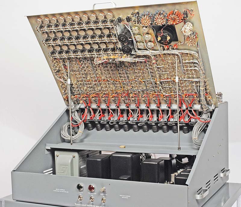
The wiring harness connecting the 364 front-panel jacks to the 15 ES-201 module connectors and the various supply modules is the single most complex assembly in the ES-400. It lives entirely on the underside of the front panel, exposed only when the panel is hinged forward.
The harness is constructed of point-to-point wire runs, each wire soldered to the rear solder lug of its corresponding banana jack and routed in bundled loom to the appropriate module connector. No printed circuit board is used for this wiring — every connection is hand-soldered in the original manufacturing process and represents a potential failure point in a sixty-year-old machine.
(reference — courtesy Nuts & Volts / David Goodsell)
Note — The Goodsell restoration documented removing the entire harness as a single unit by unscrewing all 364 jacks from the front while leaving every wire attached, thereby preserving all routing and point-to-point connections. This approach is strongly recommended: desoldering individual wires risks heat damage to adjacent connections, and the sheer density of the harness makes individual-wire tracing very difficult. After restoration work on the individual components, the harness is reinstalled by threading the jacks back through their panel holes and tightening from the front.
3.6.3 The Comparator / Bias Diode Assemblies
The ES-400 incorporates four dual bias-diode assemblies mounted on the front panel for nonlinear function generation. These are used to implement comparator-like behaviour and piecewise-linear approximations of arbitrary nonlinear functions.
Operating principle: A biased diode conducts only when the signal voltage exceeds the bias voltage. By combining several biased diodes with different bias levels and resistors, the operator constructs a piecewise-linear function approximation. This is the principle used in all analog-computer function generators of the vacuum-tube era.
The front panel page 19 of the manual illustrates the diode configuration:
   Ein ──[ R ]──┬──────────────────────── Eout
               │
          [Bias diode 1]──[Bias supply 1]
               │
          [Bias diode 2]──[Bias supply 2]
               │
              GND
Each bias supply is adjustable (set by the BIAS VOLTAGE potentiometers) and each diode conducts when the input exceeds the corresponding bias threshold, adding or subtracting current from the summing junction of a downstream amplifier. The front panel includes four dual bias-diode assemblies (tube type not confirmed in the sources). Combined with the voltage potentiometer for bias adjustment, each segment can be set independently.
Note — The exact vacuum-diode type used in the ES-400’s bias-diode assemblies is not confirmed in the available sources (the 1956 Heath brochure and Operational Manual do not state the tube type). The assemblies are described as “four dual bias-diode assemblies” in the brochure. Any small twin-diode tube of appropriate ratings would be consistent with the described function. The forward voltage drop of a vacuum diode — typically several volts at low signal currents — must be accounted for when calibrating the breakpoint voltage; the bias voltage potentiometer compensates for this drop. Detailed nonlinear function setup procedures are covered in Vol 4.
Piecewise-linear function construction: The manual (p. 23, Figure 24) shows a complete setup using the bias diode assemblies and a RAMP-FUNCTION GENERATOR configuration that produces triangle waves. By adjusting the SLOPE and BREAK VOLTAGE pots for each diode segment, arbitrary piecewise-linear approximations can be created. The ES-600 Function Generator accessory automates more complex function generation with its ten-segment diode breakpoint network.
Comparator function: When only one breakpoint is needed (i.e., a single diode and bias level), the circuit acts as a threshold detector or comparator: below threshold the diode is open and output tracks the input linearly; above threshold the diode conducts and clamps or modifies the slope. This is how the “bouncing ball” demo (Vol 4, Demo 3) reverses the sign of velocity when the ball position reaches the floor — the comparator detects the floor crossing and activates a relay or clamp.
3.6.4 The ES-505 Repetitive Oscillator and Repetitive Operation
The ES-505 Repetitive Oscillator is a separate sub-assembly (not an ES-201 module) that generates an automatic IC-OPERATE-IC cycling signal at a user-selectable rate of 0.6 to 6 Hz. It operates by driving the same relay coils that the front-panel OPERATE switch controls, overriding the manual switch with a periodic square wave. The ES-505 is enabled by the front-panel REPETITIVE ON toggle switch.
When the repetitive oscillator is active:
- For the first half of each cycle (relay energised = OPERATE), the amplifiers integrate normally.
- For the second half of each cycle (relay de-energised = IC), all integrating capacitors are recharged to their initial condition values via the IC relay contacts.
- The cycle then restarts automatically.
At 6 Hz, a complete problem runs and resets in 167 ms — fast enough to produce a nearly continuous display on an oscilloscope connected to an amplifier output jack. This is the standard technique for viewing transient or oscillatory solutions in real time. The manual’s Figure 19 (p. 17) shows an actual oscilloscope photograph of the free-fall position y(t) taken from a running ES-400 in repetitive mode.
Note — The ES-505 frequency must be chosen so the problem solution either reaches a stable endpoint or clearly reveals its character before the IC phase begins. If the problem requires 2 seconds to develop fully (e.g., a damped oscillator with time constant 1 s), set the ES-505 to 0.25 Hz or slower. The relationship between the repetition frequency and the RC time constants is a key scaling decision (Vol 4).
ES-505 operating parameters:
Table 9 — ES-505 operating parameters:
| Parameter | Value |
|---|---|
| Frequency range | 0.6–6 Hz |
| Control | Single front-panel REPETITIVE ON switch |
| Output | Drives same relay coils as OPERATE switch |
| Power | From ES-151 relay supply (2 × 50 V) |
| Resolution | Not specified in available sources; approximate dial calibration |
3.6.5 Relay Logic Integration
The two operational relays driven by the ES-151 supply are available for logical switching within a problem. Relay contacts appear as jacks on the front panel (normally open and normally closed for each relay). By feeding a comparator output (from the bias diode assembly) to the relay coil drive circuit, the operator implements an event-driven state change — effectively a one-bit binary decision inside the otherwise purely continuous analog machine.
3.7 Worked Single-Element Example: Integrating a Constant
This example traces every step from equation to verified output for the simplest useful computation on the ES-400: integrating a constant (the DC reference voltage through a coefficient pot) to produce a linearly ramping output. This constitutes the “grade school free-fall” basis demonstrated in the manual (p. 15).
3.7.1 Problem Statement
Model the position y(t) of a freely falling body, subject only to gravity, starting from rest:
  dy/dt = −g · t
  y(0) = 0
Alternatively, express as the integral of a constant acceleration a₀:
y(t) = ∫[0→t] a₀ dτ = a₀ · tSelect a₀ = 10 V/s (problem time scale 1:1, amplitude scale 10 V = 1 m/s²) and observe y(t) on the meter for the first 5 seconds.
3.7.2 Amplitude and Time Scaling
With RC = 1 s (1 MΩ input, 1 µF feedback) and a₀ = 10 V:
Eout(t) = −(1/1) × (10 V) × t = −10t [V]After 5 seconds, Eout = −50 V. This is within the ±100 V operating range, so no additional scaling is required. The sign is negative (one integrator inversion). To read a positive voltage on the meter, either accept the negative reading or insert a sign inverter after the integrator output — for this example, accept the negative sign.
3.7.3 Equipment and Patch List
Table 10 — Equipment and Patch List
| Item | Value / type |
|---|---|
| Amplifier | Any one ES-201 (e.g., amplifier 1) |
| Input resistor | 1 MΩ (plug into amp 1 input jack) |
| Feedback capacitor | 1 µF polystyrene (plug into amp 1 feedback jack) |
| Signal source | ES-50 reference +100 V jack |
| Coefficient pot | Pot 1, set to 0.10 (gives 10 V into the 1 MΩ resistor) |
| Meter | Front panel meter, METER switch → AMP ZERO first (balance), then re-route to AMPLIFIER OUTPUT |
| Patch cords | 2 cords: (1) +100 V reference → pot 1 input; (2) pot 1 wiper → amp 1 input resistor jack |
3.7.4 Step-by-Step Procedure
Step 1 — Power-up and warm-up. Apply POWER ON, then after 30 seconds apply HIGH VOLTAGE ON (manual p. 9). Allow a minimum 30-minute warm-up before precision use.
Step 2 — Balance the amplifier. Place the METER switch to AMP ZERO. Adjust the balance trimmer for amplifier 1 (labelled 1 on the front panel) until the meter reads zero. This sets the output offset of the closed-loop amplifier to zero.
Step 3 — Set the initial condition. In IC mode (OPERATE switch in IC position, relays de-energised), the integrating capacitor is discharged by the IC relay path. Confirm the amplifier 1 output reads 0 V by placing the AMPLIFIER OUTPUT switch to amplifier 1 and reading the meter. No IC supply connection is needed for zero initial condition.
Step 4 — Patch the circuit.
  +100V reference jack ──[patch cord 1]──→ Pot 1 INPUT jack
  Pot 1 WIPER jack ──[patch cord 2]──→ Amp 1 INPUT resistor (1MΩ) jack
  Amp 1 FEEDBACK jack ← 1µF capacitor (plug-in) installed
The signal path is: +100 V → attenuated by pot 1 to +10 V → flows through 1 MΩ into summing junction → amplifier integrates → output ramps negatively.
Step 5 — Set the coefficient. Switch METER to POT READ. Connect a patch cord from the +100 V reference to pot 1 input and pot 1 wiper to the meter input jack. Adjust pot 1 until the meter reads exactly +10.0 V. This confirms a coefficient of 0.100.
Step 6 — Run. Throw the OPERATE switch. The relays energise, disconnecting the IC path and connecting the integration path. The output of amplifier 1 begins ramping from 0 V toward negative values at a rate of 10 V per second.
Step 7 — Read and verify. With METER connected to AMPLIFIER OUTPUT for amplifier 1, observe the meter needle sweeping from 0 V toward −20 V (near full scale for the ±20 V meter range) in approximately 2 seconds. After 5 seconds, the output will be at −50 V.
Expected values vs. time:
Table 11 — Expected values vs. time:
| Time (s) | Expected output (V) | Meter reading |
|---|---|---|
| 0 | 0.0 | 0.0 |
| 1 | −10.0 | −10.0 |
| 2 | −20.0 | −20.0 (near FSD) |
| 5 | −50.0 | Offscale on ±20 V range |
| 10 | −100.0 | Saturation — NE-51 lights |
Note — At t = 10 s the output reaches −100 V and saturates. The NE-51 neon indicator on amplifier 1 illuminates. Throw the OPERATE switch back to IC to reset. For the purposes of this demonstration, simply observe the ramp for the first 2 seconds or connect an oscilloscope to the amplifier output jack to observe beyond the meter’s ±20 V range.
Step 8 — Repetitive mode (optional). The ES-505 Repetitive Oscillator (0.6–6 Hz range) can drive the OPERATE relay automatically, resetting and re-running the integration at a user-selected rate. With an oscilloscope connected to amplifier 1’s output jack and the oscilloscope’s time base triggered by the ES-505 output, the ramp waveform is displayed continuously. This is the standard technique for observing short-duration transients.
3.7.5 Signal-Flow Diagram
  ┌──────────────┐    10 V     ┌─────────────────────────────┐
  │ ES-50 +100V  │─────────────│ Pot 1 (coeff = 0.10)        │
  │ reference    │ patch cord 1│                              │
  └──────────────┘             └──────────────┬──────────────┘
                                              │ 10 V (attenuated)
                                              │ patch cord 2
                               ┌──────────────▼──────────────┐
                               │ R = 1 MΩ  [input resistor]  │
                               │            ↓                 │
                               │      [Σ summing junction]   │
                               │            ↓                 │
                               │    ES-201 amplifier 1        │
                               │    gain ≈ 50,000             │
                               │            ↓                 │
                               │    C = 1 µF [feedback cap]  │
                               └──────────────┬──────────────┘
                                              │
                                              ▼
                                     Eout = −10·t  [V]
                                     (linear ramp, 10 V/s)
                                              │
                                              ├──→ front-panel meter
                                              └──→ oscilloscope
3.7.6 Oscilloscope Observation
Connecting an oscilloscope to the amplifier output jack during the worked example reveals additional information not available from the front-panel meter:
-
Linearity check: The ramp should appear as a straight line on the oscilloscope time base. Any curvature indicates integrator error — the most common cause is a dielectric absorption transient at the start of the run (the capacitor “remembers” the previous run’s endpoint).
-
IC settling: In repetitive mode, the transition from the IC phase back into integration appears as a sharp voltage step followed by the linear ramp. If the step has a ringing or exponential tail, it suggests either the IC relay contacts are bouncing, or the IC voltage supply is not well filtered.
-
Gain accuracy: After a 10-second run (if not saturated), the output should be exactly −100 V with the given component values. Any deviation indicates either the pot is not exactly at 0.10, the resistor or capacitor values deviate from nominal, or the amplifier is introducing gain error.
The oscilloscope connection for repetitive-mode display is illustrated in the manual (p. 11, Figure 11): vertical input to the amplifier output jack, horizontal either to an internal time base (normal mode) or to the ES-505 oscillator output for phase-synchronised display.
(reference — courtesy Nuts & Volts / David Goodsell)
3.7.7 What Can Go Wrong — Troubleshooting Triage
Table 12 — What Can Go Wrong — Troubleshooting Triage
| Symptom | Likely cause | Remedy |
|---|---|---|
| Output stuck at 0 V in OPERATE | IC relay contacts welded closed; or capacitor open | Check relay operation; measure capacitor continuity |
| Output drifts before OPERATE switch is thrown | IC relay contacts not seating; capacitor leakage | Replace relay contacts; replace capacitor with polystyrene type |
| Ramp rate is wrong (too fast/slow) | R or C value incorrect; pot not set correctly | Measure R and C with LCR meter; re-verify pot setting with POT READ |
| Ramp direction is positive (not negative) | Input signal polarity inverted; or wrong reference jack used | Check reference: +100 V jack, not −100 V |
| Output immediately saturates (+100 V or −100 V) | Amplifier not balanced; feedback capacitor shorted | Re-run balance procedure; verify capacitor is not shorted |
| NE-51 lights immediately | Output at rail; same as above | Same as above |
| Meter reads zero in POT READ even with signal applied | Patch cord from pot wiper to meter input not installed | Add patch cord |
3.8 ES-400 vs. EC-1 — Computing Element Comparison
The Heathkit EC-1 is the smaller desktop companion computer (nine ES-201 amplifiers, same tube types, same ±100 V signal range). Understanding the differences helps when the EC-1 manual is used as a secondary reference for ES-400 operation.
Table 13 — ES-400 vs. EC-1 — Computing Element Comparison
| Feature | ES-400 | EC-1 |
|---|---|---|
| Number of ES-201 op-amp modules | 15 | 9 |
| Total banana-plug jacks | 364 | ~150 (estimated) |
| Coefficient potentiometers (standard) | 30 | 18 |
| Auxiliary 10-turn pots | 2 | 1 |
| Operational relays | 2 | 1 |
| IC power supplies (ES-100 modules) | 3 (six channels) | 1 (two channels) |
| ES-505 repetitive oscillator | Yes | Yes |
| ES-600 function generator | Optional accessory | Not supported |
| Bias diode assemblies | 4 (four dual-diode units) | 2 |
| Front-panel meter | 1 × DC milliammeter | 1 × DC milliammeter |
| Cabinet style | Floor-standing console, 168 lb | Desktop case |
| Tube count (op-amps only) | 45 (15 × 3) | 27 (9 × 3) |
| Original price | $945 (Group C) | ~$200 (estimated) |
The EC-1 operation manual (freely available from the Analog Computer Museum) contains extended theory sections and worked examples entirely applicable to the ES-400; the circuit topologies and component values are identical. The only difference the operator must account for is the larger number of available amplifiers in the ES-400.
3.9 Computing-Element Component Bill of Materials (Restoration BOM)
The following table covers the passive computing components — those that are plug-in or soldered to the ES-201 PCBs and that the restorer should plan to replace. Power supply capacitors and the ES-2 rectifier components are covered in Vol 5.
Table 14 — Computing-Element Component Bill of Materials (Restoration BOM)
| Component | Location | Spec (original) | Recommended replacement | Qty per ES-201 | Total (15 modules) |
|---|---|---|---|---|---|
| 12AX7 dual triode | ES-201 socket V1 | GE, Sylvania, or RCA original | Chinese new-production (TubesAndMore.com, ~$9.59 ea) | 1 | 15 |
| 6BQ7 dual triode | ES-201 socket V2 | GE, Sylvania original | Vintage NOS (eBay); also 6BQ7A acceptable | 1 | 15 |
| 6BH6 sharp-cutoff pentode | ES-201 socket V3 | Any major brand | Vintage NOS (eBay); common IF amplifier tube | 1 | 15 |
| NE-51 neon indicator | ES-201 PCB | NE-51 standard | New NE-51 from any electronics supplier | 1 | 15 |
| 9-pin noval socket (V1, V2) | ES-201 PCB | Phenolic or ceramic | Ceramic 9-pin noval (Mouser/Digi-Key) | 2 | 30 |
| 7-pin miniature socket (V3) | ES-201 PCB | Phenolic or ceramic | Ceramic 7-pin (Mouser/Digi-Key) | 1 | 15 |
| Carbon comp resistors | ES-201 PCB | Various values, 0.5 W | 1% metal-film (Mouser/Digi-Key), 0.5 W | ~12 | ~180 |
| Electrolytic capacitors | ES-201 PCB | Various µF, 350–450 V | High-voltage axial electrolytic (TubesAndMore.com) | ~4 | ~60 |
| Paper/mica bypass caps | ES-201 PCB | 100–500 pF | Silver mica or C0G ceramic (Mouser) | ~6 | ~90 |
| Integration capacitors (plug-in) | Computing field (plug-in) | 1 µF, 0.1 µF polystyrene | Polystyrene film (CDE/Vishay); polyethylene acceptable | 1–3 per setup | As needed |
| Input resistors (plug-in) | Computing field (plug-in) | 1 MΩ, 0.1 MΩ 1% | 1% metal film (Mouser/Digi-Key) | 1–5 per setup | As needed |
| Feedback resistors (plug-in) | Computing field (plug-in) | 1 MΩ, 10 MΩ 1% | 1% metal film | 1 per summer | As needed |
Note — The “plug-in” computing resistors and capacitors are inserted directly into banana jacks and must have leads formed to banana-plug size or be mounted on small plug-in adapters. The original ES-400 was supplied with a component set designed for this purpose; reproduction sets can be fabricated by soldering component leads to short sections of 2 mm banana plug shaft stock.
3.10 Propagation Delay and Bandwidth Considerations
Unlike digital computers, the ES-400’s computation is fundamentally continuous and real-time. However, the vacuum-tube stages do introduce finite signal bandwidth and propagation delay that matter when very fast input transients are applied.
The 6BH6 output pentode stage, operating in class A with a resistive load, has a bandwidth of roughly 100 kHz in typical tube-amplifier configurations. The closed-loop bandwidth of the ES-201 with unity feedback is approximately:
f_cl ≈ A × f_unity_loop ≈ (gain × bandwidth product) / feedback_factorFor a summer with gain = 1, the closed-loop bandwidth is on the order of tens of kilohertz — more than adequate for the DC-to-10 Hz signals that dominate analog computer problems. For an integrator with 1 MΩ / 1 µF (RC = 1 s), the unity-gain integrator crossover is at 1/(2π × RC) = 0.16 Hz, and the amplifier’s excess gain far exceeds unity well into the kilohertz range.
In practice, the bandwidth of the ES-400 computing chain is not a limitation for any of the problems the machine was designed to solve. The ES-505 repetitive oscillator operates at ≤ 6 Hz; even with fifth-harmonic content at 30 Hz, the amplifier chain reproduces waveforms faithfully.
Note — When connecting modern function generators or signal sources to the ES-400 input jacks, the signal amplitude must be scaled to remain within ±100 V. A standard function generator output of ±10 V can be connected directly to a pot input and the pot set to 1.0 for full-amplitude injection, or the generator can be set for its ±100 V-capable output range if available. See also Vol 4 for signal interface details.
3.11 Cross-References
- Vol 1 — History, physical description, sub-assembly inventory, production context.
- Vol 2 — Power supply chain: ES-2 amplifier supply, ES-50 reference supply, ES-100 IC supplies, ES-151 relay supply.
- Vol 4 — Problem scaling, block diagram construction, multi-amplifier programs, the harmonic oscillator, spring-mass-damper, and other standard setups. The coefficient scaling trees introduced here are worked out quantitatively in Vol 4.
- Vol 5 — Restoration: capacitor selection, tube replacement, front-panel cleaning, amplifier rebalancing after recapping.
3.12 Summary Tables
3.12.1 Computing-Element Quick Reference
Table 15 — Computing-Element Quick Reference
| Element | Config | Transfer function | Key components |
|---|---|---|---|
| Sign inverter | Summer, gain = −1 | Eout = −Ein | Rin = Rfb = 1 MΩ |
| Weighted summer | Summer, N inputs | Eout = −Σ(Rfb/Rn)·En | Rin1…RinN, Rfb |
| Integrator | Capacitor feedback | Eout = −(1/RC)∫Ein dt | Rin = 1 MΩ, Cfb = 1 µF (typical) |
| Scaled integrator | Integrator + pot | Eout = −(k/RC)∫Ein dt | k = pot coefficient 0–1 |
| Sign + scale | Summer, unequal R | Eout = −(Rfb/Rin)·Ein | Rfb ≠ Rin |
| Comparator/clamp | Bias diode | Eout ≈ Ein for Ein < Vbias; clamped beyond | Bias diode + adjustable supply |
3.12.2 Patch Cord Signal Levels
Table 16 — Patch Cord Signal Levels
| Signal type | Typical range | Notes |
|---|---|---|
| Computing signal | ±100 V | Op-amp output; load > 10 kΩ |
| Reference (+100 V) | +100.0 V ± 0.1% | From ES-50; high-precision rail |
| Reference (−100 V) | −100.0 V ± 0.1% | From ES-50 |
| IC supply (floating) | 0–100 V floating | From ES-100; never ground the common |
| Attenuated coefficient | 0–±100 V | Pot wiper output |
| Meter input | ±20 V FS | Panel meter range |
| Oscilloscope output | ±100 V | Same as computing signal; use ÷10 probe |
3.12.3 NE-51 Overload Indicator Key
Table 17 — NE-51 Overload Indicator Key
| Indicator state | Meaning | Action |
|---|---|---|
| Off | Output within ±100 V; normal operation | None |
| Illuminated during OPERATE | Output saturated at ±100 V | Return to IC; revise amplitude scaling |
| Illuminated during IC | Amplifier not balanced; or IC voltage > 100 V | Re-balance; check IC supply setting |
| Flickering | Near-saturation transient; marginal scaling | Increase amplitude scale factor by 2× |
| Always on, any mode | Amplifier fault; tube failure | Remove module; check 6BH6 output stage |
Volume 3 — Computing elements & patchbay. Sources: Heath Electronic Analog Computer Operational Manual (Heath Company, Benton Harbor, MI); ES-400-Research.md compiled 2026-04-12; Goodsell, David, “Restoring the Heathkit ES-400 Computer,” Nuts & Volts, 2019.
Comments (0)