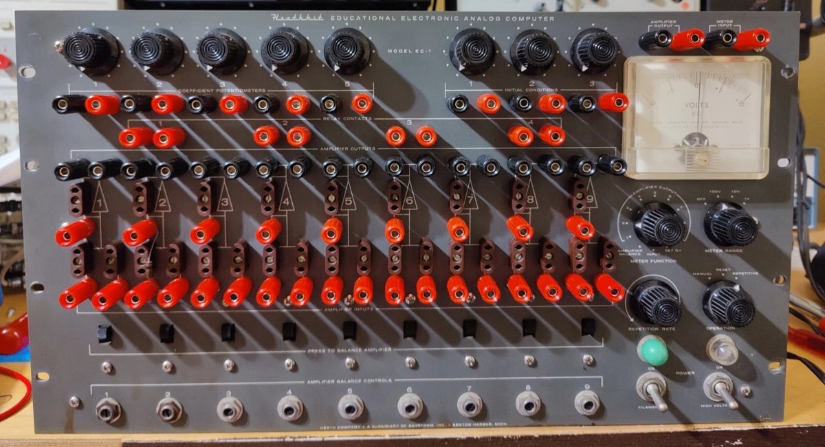
Heathkit EC-1 · Volume 7
Heathkit EC-1 — Volume 7 — Modern extensions & interfacing
Solid-state substitution, data-logging, bench-supply alternatives, patch hardware, and reversibility discipline — bridging 1959 silicon-free design to modern instrumentation
7.1 About this Volume
The Heathkit EC-1 was engineered in a world without op-amp ICs, USB data acquisition, switching regulators, or 3.3 V microcontrollers. Its signal rails swing ±60 V; its plate-supply rails reach +300 V; its sole time-base is a mechanical relay or a multivibrator that tops out at 15 cycles per second. Every one of those facts creates an interface challenge when connecting the machine to twenty-first-century instrumentation.
This volume addresses four practical classes of modernization:
- Solid-state amplifier substitution — when and whether to replace the nine 6U8-based DC op-amps with IC equivalents, and what the tradeoffs are.
- Data-logging the output — safe, calibrated attenuation of the ±60 V signal rails into ADC-friendly levels, USB-DAQ capture, and oscilloscope connection.
- Bench-supply substitution — replacing or augmenting the internal +300 V / −150 V / heater rails with external regulated supplies during development or fault-finding.
- Patch-cord and jack hardware — sourcing, fabricating, and documenting the banana-jack ecosystem and the two-pin component plugs that are no longer manufactured.
A fifth section addresses the ethics and practice of reversibility: every modification described here can be undone, leaving the original chassis intact for a future curator.
Cross-references: amplifier circuit theory and power-supply circuit detail are developed in Vol 2; patch panel and computing elements are in Vol 3; restoration procedure sequence is in Vol 4; oscilloscope programming setups are in Vol 5.
Note — The EC-1 output jacks are the only safe connection points for any external equipment. The +300 V plate bus, the −150 V regulated rail, and the heater wiring are internal, unguarded, and lethal. Nothing in this volume authorizes probing inside a powered chassis without the explicit isolation procedure described in §6.
7.2 Solid-State Amplifier Substitution
7.2.1 Why the Question Arises
Nine 6U8 pentode-triode tubes form the core of every EC-1 op-amp. The 6U8 is still manufactured (JJ Electronic, Electro-Harmonix) and is widely available as new-old-stock. Nevertheless, restorers occasionally ask whether a single-chip substitute — an OPA2134, LT1013, or AD711 — could replace the tube stage, either to extend service life, reduce heat, or demonstrate the conceptual equivalence of the two technologies.
The answer is nuanced: substitution is feasible for low-voltage demonstration rigs, but a fully transparent drop-in that preserves the original ±60 V swing on the original ±300 V / −150 V rails is considerably more complex than it first appears.
7.2.2 The 6U8 Op-Amp Circuit — What Must Be Matched
Each EC-1 amplifier section comprises a triode input stage (one half of the 6U8) driving a pentode output stage (the other half), with overall negative feedback closing through the problem-board resistor network. Key parameters that an IC substitute must match or exceed:
Table 1 — Each EC-1 amplifier section comprises a triode input stage (one half of the 6U8) driving a pentode output stage (the other half), with overall negative feedback closing through the problem-board resistor network. Key parameters that an IC substitute must match or exceed
| Parameter | 6U8 Tube Circuit | Requirement for Substitution |
|---|---|---|
| Open-loop gain | ~1,000 (60 dB) | ≥ 60 dB (easily met by any modern op-amp) |
| Output voltage swing | ±60 V (at ±300 V / −150 V rails) | Requires HV op-amp rated ≥ ±65 V supply |
| Output current | 0.7 mA continuous | 0.7 mA minimum; most HV ICs can do 10–25 mA |
| −1 dB bandwidth | 600 Hz | Trivially met; even legacy 741 is 1 MHz |
| Input bias current | Very low (grid draws ~0 in normal operation) | ≤ 1 nA preferred to avoid resistor-induced offset |
| Offset voltage | Nulled by 3 kΩ balance pot | ≤ ±5 mV so pot range suffices |
| Noise | Not specified; tube noise dominates at HF | VHF noise irrelevant; 1/f noise in EC-1’s audio band |
| Thermal drift | ~1 mV/°C after warm-up | Match or better |
| Supply rejection | Moderate (VR-tube regulated rails) | ≥ 60 dB PSRR adequate |
The critical constraint is output swing: the problem board is designed around ±60 V, and all resistor plug values, scaling, and initial-condition voltages are calculated for that range. A ±15 V swing substitute would require rescaling every coefficient by a factor of four — effectively rebuilding the problem library from scratch.
7.2.3 Candidate ICs for ±60 V Operation
Very few monolithic op-amps tolerate supply voltages approaching ±75 V (the minimum overhead needed). The two credible families are:
Table 2 — Very few monolithic op-amps tolerate supply voltages approaching ±75 V (the minimum overhead needed). The two credible families are
| Part | Manufacturer | Max Supply (±V) | Typical Vout swing | Ibias | Notes |
|---|---|---|---|---|---|
| PA85 | Apex Microtechnology | ±150 V | ±(Vs − 5 V) | 50 pA | Discrete HV op-amp; expensive (~$60) |
| OPA445 | Texas Instruments | ±45 V | ±(Vs − 2 V) | 10 pA | Only ±45 V — insufficient for ±60 V swing |
| OPA452 | Texas Instruments | ±40 V | ±(Vs − 2 V) | 5 nA | Insufficient supply headroom |
| LTC6090 | Analog Devices | ±70 V (140 V total) | Rail − 1.5 V | 5 pA | Strong candidate; ~$12; DIP-8 available |
| ADHV4702-1 | Analog Devices | ±110 V | ±(Vs − 15 V) | 3 pA | Very wide supply; limited availability |
| PA88 | Apex | ±175 V | ±(Vs − 5 V) | 20 pA | Highest headroom; most expensive |
The LTC6090 from Analog Devices is the most practical single-chip choice: it operates from total supplies up to 140 V (i.e., +70 V / −70 V), can swing to within 1.5 V of each rail, and is available in DIP-8 for through-hole prototyping. With the EC-1’s +300 V / −150 V rails stepped down to a symmetric ±70 V auxiliary supply derived from a small dropping regulator, an LTC6090 can replicate the tube amplifier’s transfer function. The Apex PA85 is the premium option if the dropping-regulator approach is objectionable.
7.2.4 Substitution Architecture
A direct drop-in is mechanically impossible: the 6U8 is a 9-pin Noval tube; there is no pin-compatible IC. Any substitution requires a daughter board that fits into the tube socket, presents the correct heater-current load to the transformer (or bypasses the heater supply), and provides the op-amp function at the correct voltage.
┌─────────────────────────────────────────────────────────────────┐
│              SUBSTITUTION DAUGHTER BOARD (schematic concept)    │
│                                                                 │
│   9-pin Noval plug  ──►  Pin 1 (plate / output)  ──────────────┤──► Vout
│                          Pin 2 (control grid)    ──────────────┤──► V−
│                          Pin 9 (cathode)         ──────────────┤──► V+
│                          Pins 4,5 (heaters)      ──► 6.3 VAC   │
│                                                                 │
│   On-board: LTC6090 + ±70 V drop regulators                    │
│             Offset trim pot (replaces balance pot function)     │
│             Thermal relief resistors in supply path             │
└─────────────────────────────────────────────────────────────────┘
The heater pins (4 and 5) should present the correct 6.3 V / 0.9 A load to keep the heater transformer in regulation — either by connecting a dummy 7 Ω / 6 W wirewound resistor across those pins, or by powering the daughter board from the heater winding through a bridge rectifier and small regulator.
7.2.5 What Is Lost in Substitution
Even a technically competent solid-state substitution sacrifices several authentic properties:
Table 3 — Even a technically competent solid-state substitution sacrifices several authentic properties
| Loss | Engineering Impact | Aesthetic Impact |
|---|---|---|
| Tube warm-up drift (2–5 min) | Faster availability; computation begins at once | No warm-up ritual |
| Purple glow of OA2/OB2 VR tubes | Unaffected (those remain) | Minor |
| 6U8 visual glow | Nine dark sockets | Significant for demonstration |
| Authentic 60-year-old noise floor | IC noise is lower; small discrepancy in published setups | Subtle |
| Period-correct bandwidth limitation (600 Hz −1 dB) | IC bandwidth is far wider; some published demo setups rely on rolloff | Possible accuracy change in high-speed repetitive mode |
| Originality for museum / appraisal | Significantly reduced | Major for collectors |
Note — The 600 Hz bandwidth is not a nuisance; it is a deliberate design constraint that prevents parasitic oscillation in high-gain configurations on the original resistor-network problem board. An unconditionally stable HV op-amp with megahertz bandwidth may oscillate if installed without compensation. A 600 Hz single-pole roll-off (RC = 265 µs) should be added at the IC’s compensation pin or in a feedback capacitor to preserve stability in all documented problem setups.
7.2.6 Recommendation
For a working restoration intended for programming demonstrations, keep the 6U8 tubes. They are available, they balance easily with the original 3 kΩ trim pots, and they define the machine. For an educational electronics project — where the goal is specifically to compare tube and IC op-amp behavior — a reversible daughter-board substitution using the LTC6090 is the most practical approach. Document every modification and retain the original tubes.
Tip — A useful middle path is to build a standalone ±60 V IC op-amp module on a separate breadboard, patch it in parallel with one EC-1 amplifier, and compare outputs. This demonstrates the equivalence without touching the chassis at all.
7.3 Data-Logging the Output
7.3.1 The Voltage-Level Problem
The EC-1’s front-panel output binding posts swing between approximately −60 V and +60 V, relative to the computer’s signal ground (the black binding posts). Every modern ADC, oscilloscope input on the ×1 range, microcontroller ADC, and USB data-acquisition module operates at voltages between −10 V and +10 V at best; most single-supply embedded ADCs accept only 0 to 3.3 V or 0 to 5 V.
Direct connection of the EC-1 output to modern low-voltage hardware will destroy the hardware. A precision attenuation and level-shifting interface is mandatory.
7.3.2 Ground Reference Warning
Danger — The EC-1’s signal ground is the chassis ground, which is connected to the AC safety earth through the three-conductor power cord. USB-DAQ devices, oscilloscopes, and laptops each have their own chassis ground, also earth-connected. If the EC-1 signal ground and the instrument ground are at different potentials — for example, because the EC-1 is on an isolation transformer — a ground loop forms that may damage inputs. Before connecting any external instrument, verify that both the EC-1 and the instrument share the same AC outlet strip or that an appropriate differential input is used.
7.3.3 Resistive Voltage Divider (Simplest Method)
A two-resistor voltage divider can scale ±60 V down to a safe level. For a 0 to +3.3 V ADC with a mid-supply bias, a three-resistor network that adds a +1.65 V offset is required. A simpler approach targets ±10 V for instruments with bipolar inputs:
Divider for ±60 V → ±5 V (ratio 1:12):
EC-1 output (+/-60 V)
       │
      [R1: 110 kΩ, 1%, 0.5 W metal film]
       │
       ├──────────────────────────────► To ADC or scope (±5 V)
       │
      [R2: 10 kΩ, 1%, 0.25 W]
       │
    EC-1 GND (black binding post)
Attenuation ratio: R2 / (R1 + R2) = 10 / 120 = 1/12 → ±5 V output for ±60 V input.
The output impedance of this divider is R1 ∥ R2 = 9.17 kΩ. This is acceptable for scope inputs (≥1 MΩ) but problematic for ADC inputs with sample-and-hold circuits that draw short current pulses. An op-amp buffer is strongly recommended.
Danger — The resistors in the divider must be rated for the maximum voltage across them: R1 sees up to 55 V under worst-case conditions. Use 0.5 W metal-film parts with a 200 V (or higher) voltage rating. Standard 1/4 W carbon resistors rated 50–75 V must not be used here.
7.3.4 Buffered Attenuator Interface Board
The recommended interface uses a precision resistor divider followed by a unity-gain buffer amplifier. A single-supply op-amp (such as the OPA2134 or TL072) powered from a USB-derived ±15 V module handles this cleanly.
Interface block diagram:
7.3.5 Component Bill of Materials — Attenuator Board
Table 4 — 3.5 Component Bill of Materials — Attenuator Board
| Reference | Part | Value / Part Number | Qty | Source | Approx Cost |
|---|---|---|---|---|---|
| R1 | Metal-film resistor | 110 kΩ, 1%, 0.5 W, 250 V | 1 per channel | Digi-Key MFR-25FBF52-110K | $0.15 |
| R2 | Metal-film resistor | 10 kΩ, 1%, 0.25 W | 1 per channel | Digi-Key MFR-25FBF52-10K | $0.10 |
| U1 | Dual op-amp | OPA2134UA (or TL072) | 1 (2 channels) | Digi-Key OPA2134UA/2K5 | $3.50 |
| D1, D2 | Schottky clamp | BAT54S (SOT-23 dual) | 1 per channel | Digi-Key BAT54SFILM-ND | $0.30 |
| PS1 | DC-DC converter | Traco TMA 1515D (±15 V, 1 W) | 1 | Digi-Key 1034-1045-ND | $9.00 |
| J1–J4 | Banana jacks | Red/black panel-mount | 4 | Digi-Key J161-ND | $1.50 ea |
| J5, J6 | BNC or SMA jacks | Panel-mount, 50 Ω | 2 | Mouser 523-31-221-RFX | $2.00 ea |
| PCB | Perfboard | 0.1” pitch, 3×4 in | 1 | Amazon or Digi-Key | $2.00 |
Total BOM cost (two channels, single board): approximately $25–30.
7.3.6 Scope Connection — Direct via 10× Probe
The simplest capture method requires no additional hardware: a standard 10× oscilloscope probe has a built-in 9 MΩ series resistor that, combined with the scope’s 1 MΩ input, creates a 10:1 divider. With a 10× probe, the scope displays 1 V per actual volt; at 60 V full scale the scope reads 6 V, well within the 10 V/div capability of any modern instrument.
Probe connection at the EC-1: Use a banana-to-grabber adapter (Pomona part 3782-0 or equivalent). Clip the ground lead to an EC-1 black binding post; clip the probe tip to the output red post of the amplifier under observation.
Table 5 — 3.6 Scope Connection — Direct via 10× Probe
| Scope Setting | Value | Note |
|---|---|---|
| Coupling | DC | AC coupling blocks the slowly varying DC signals |
| V/div | 10 V/div (×10 probe reads 100 V/div actual) | Shows ±60 V in ~6 divisions |
| Probe attenuation setting | ×10 | Must be set on scope, not just physically attached |
| Time base | 0.1–10 s/div | EC-1 repetitive rate 0.1–15 Hz |
| Input impedance | 1 MΩ | Standard; do not use 50 Ω input |
Danger — Do not connect the oscilloscope’s ground clip (shield of BNC, chassis of probe) to any EC-1 terminal other than the signal ground (black binding posts). The EC-1’s internal HV rails are not connected to the front-panel binding posts, but accidental contact during probing is possible if the chassis is open. Ground the oscilloscope and the EC-1 to the same AC outlet before connecting probes.
7.3.7 USB Data-Acquisition Capture
After passing through the attenuator board (§3.4), the ±5 V signal can be connected to any general-purpose USB-DAQ. Two well-suited devices:
Table 6 — After passing through the attenuator board (§3.4), the ±5 V signal can be connected to any general-purpose USB-DAQ. Two well-suited devices
| Device | Channels | Sample Rate | Resolution | OS | Cost |
|---|---|---|---|---|---|
| Measurement Computing USB-1208FS | 8 SE / 4 diff | 50 kS/s | 12-bit | Win/Mac/Linux | ~$180 |
| National Instruments USB-6001 | 8 AI (±10 V) | 20 kS/s | 14-bit | Win/Mac/Linux | ~$220 |
| Digilent MCC 118 (Raspberry Pi HAT) | 8 SE | 100 kS/s | 12-bit | Linux/RPi | ~$99 |
| Arduino Uno (with divider only) | 6 AI | 9.6 kS/s | 10-bit (0–5 V) | Any | ~$25 |
The EC-1’s useful signal bandwidth is 600 Hz (−1 dB point). Even the slowest USB-DAQ listed above (20 kS/s) satisfies Nyquist by a factor of 16. Sample at 2,000 S/s for typical logging; increase to 10,000 S/s for repetitive-mode X-Y capture.
A Python snippet for continuous logging using MCC’s mcculw library:
# Requires mcculw (pip install mcculw) and MCC USB-1208FS
from mcculw import ul
from mcculw.enums import ULRange
import time, csv

BOARD = 0; CHAN = 0; RANGE = ULRange.BIP5VOLTS

with open("ec1_log.csv", "w", newline="") as f:
    writer = csv.writer(f)
    writer.writerow(["t_s", "v_out_V", "v_scaled_V"])
    t0 = time.time()
    while True:
        raw = ul.a_in(BOARD, CHAN, RANGE)
        volts_adc = ul.to_eng_units(BOARD, RANGE, raw)
        # Invert attenuation factor (12×) to recover true EC-1 voltage
        volts_ec1 = volts_adc * 12.0
        writer.writerow([f"{time.time()-t0:.4f}", f"{volts_adc:.5f}", f"{volts_ec1:.3f}"])
        time.sleep(0.001)  # 1 ms → 1 kS/s effective rate
Captured data can be plotted with matplotlib or imported into MATLAB / Octave for comparison against the analytical solution of the simulated differential equation.
7.3.8 Calibration of the Interface
Before trusting logged data, calibrate the attenuator chain against a known reference:
- Apply a known DC voltage from a bench supply (e.g., +30.00 V verified with a 4.5-digit DMM) to the EC-1 output binding posts.
- Record the ADC reading in software.
- Compute actual attenuation ratio: ratio = V_reference / V_adc.
- Apply ratio as a scalar correction factor in the logging script.
- Repeat at −30.00 V to check for asymmetry (indicates op-amp offset or divider mismatch).
Typical residual error after calibration: ±0.5% (limited by 1% resistors and op-amp offset).
7.4 Bench-Supply Substitution for the ±300 V and Heater Rails
7.4.1 When Substitution Is Appropriate
The EC-1’s internal power supply is adequate for normal operation, but three scenarios motivate substitution or augmentation with bench supplies:
- Fault-finding during restoration — before the internal supply is verified, an external regulated supply allows safe stepwise energization of individual amplifier stages.
- Heater transformer failure — the 6.3 VAC heater winding is wound on a bespoke transformer; if it opens, an external 6.3 V / 10 A AC supply (or regulated DC for DC-heated substitution) can restore operation while a replacement transformer is sought.
- Teaching circuit behavior — intentionally varying the B+ voltage while observing output offset illustrates power-supply rejection; an external supply makes this safe and adjustable.
7.4.2 Internal Supply Summary
The EC-1 internal supply produces four distinct voltages that are all essential to operation:
Table 7 — The EC-1 internal supply produces four distinct voltages that are all essential to operation
| Rail | Nominal | Regulation | Current | Purpose |
|---|---|---|---|---|
| +300 V (B+) | +300 V DC | Electronic series-pass regulator (adjustable +250 to +350 V) | 25 mA max | Plate supply for all nine 6U8 op-amps and multivibrator |
| −150 V (B−) | −150 V DC | Single OA2 VR tube (150 V regulation) | 40 mA max | Negative plate / bias supply |
| +100 V (IC) | +100 V DC (×3) | OB2 VR tube regulated (108 V); capacitor-filtered | Low (IC circuits only) | Initial-condition supplies for three integrators |
| 6.3 VAC | 6.3 V AC | Transformer secondary (unregulated) | ~9 A total (9 × ~0.9 A heaters + misc) | All tube heaters |
7.4.3 External B+ Supply Requirements
A replacement or supplemental +300 V supply must satisfy:
- Output voltage: Adjustable from +250 to +350 V DC (to allow gradual forming of old electrolytic capacitors per the variac procedure described in Vol 3).
- Current capacity: 50 mA minimum (25 mA for the EC-1 plus margin).
- Regulation: < 1% load regulation from 5 to 25 mA load.
- Ripple: < 50 mV peak-to-peak (the EC-1’s own regulated supply achieves ~20 mV; excess ripple appears as 120 Hz noise on all amplifier outputs).
- Short-circuit protection: Essential; a wiring error during development could short B+ to chassis.
- Output impedance: < 100 Ω at 120 Hz (to maintain regulation against heater-induced modulation).
Recommended external HV supply options:
Table 8 — Recommended external HV supply options:
| Supply | Vout Range | Iout | Notes | Cost |
|---|---|---|---|---|
| Agilent / Keysight N5752A | 0–600 V | 0–1.25 A | Lab-grade; complete protection | ~$800 used |
| BK Precision 1787B | 0–500 V | 0–120 mA | Adequate for EC-1; affordable | ~$350 new |
| Matsusada AU-300P1 | 0–300 V | 0–1 A | Japanese; well regarded | ~$500 new |
| DIY tube rectifier supply | +250–+350 V | 50 mA | EL34/6L6-based; period-correct | Parts ~$80 |
| Rod Elliott P39 CRC supply | Adjustable | 100 mA | PCB available; solid-state | Parts ~$60 |
Danger — Any bench supply delivering +300 V must have its output connected to the EC-1 through a series 1 kΩ / 5 W current-limiting resistor during initial power-up (forming procedure). Remove the resistor only after verifying that current draw is stable and within spec. Touching a 300 V output terminal delivers a potentially lethal shock. Keep one hand in a pocket; work with insulated probes only.
7.4.4 External −150 V Supply
The negative supply provides −150 V at up to 40 mA. A bench supply set to −150 V with 50 mA current limit is adequate. Most variable benchtop HV supplies are unipolar; a second supply floated above ground achieves a negative rail. Alternatively, the DC-DC converter approach using an isolated −150 V module (e.g., Emco CA150) suffices for lower-current testing.
The OA2 and OB2 VR tubes in the original supply are the most visually dramatic components in the EC-1; their purple glow is part of the machine’s identity. If the original supply is functional, there is rarely a reason to substitute the negative rail.
7.4.5 Heater Supply Substitution
The 6.3 VAC heater supply feeds nine 6U8 tubes plus the 6AQ5, 12BH7, and 6BH6. Total heater current:
Table 9 — The 6.3 VAC heater supply feeds nine 6U8 tubes plus the 6AQ5, 12BH7, and 6BH6. Total heater current
| Tube | Qty | Heater (V/A) | Subtotal (A) |
|---|---|---|---|
| 6U8 | 9 | 6.3 V / 0.45 A | 4.05 A |
| 6AQ5 | 1 | 6.3 V / 0.45 A | 0.45 A |
| 12BH7 | 1 | 12.6 V / 0.30 A (wired as 6.3 V parallel) | 0.60 A |
| OA2 | 1 | 6.3 V / 0.30 A | 0.30 A |
| OB2 | 1 | 6.3 V / 0.30 A | 0.30 A |
| 6BH6 | 1 | 6.3 V / 0.30 A | 0.30 A |
| Total | 14 | ~6.0 A |
A standard 6.3 V / 8 A toroidal transformer (Antek AN-0508 or Hammond 166F6) can replace the original heater winding if the primary transformer is damaged. DC heating (6.3 V DC regulated) eliminates 60 Hz hum coupling into the cathode circuits and is used in premium audio restorations; 6.3 V DC at 6 A requires a robust 40 W linear or switching regulator.
Tip — When substituting the heater supply with DC, apply it in series with a 10 Ω resistor for the first power-on. Tube heaters have a cold resistance approximately 1/5 of their hot resistance; the inrush current at power-on can reach 5× the steady-state value. The series resistor limits inrush and protects both the supply and the tube heaters. Remove it after warm-up if operating temperature stability is a concern.
7.4.6 Power Tree — Complete EC-1 Supply Architecture
┌─────────────────────────────────────────────────────────────────────────────┐
│                    EC-1 POWER DISTRIBUTION TREE                             │
│                                                                             │
│  105–125 VAC ──┬── Main ON/OFF switch                                       │
│  50/60 Hz      │                                                            │
│                ▼                                                            │
│         Power transformer                                                   │
│         (bespoke, ~100 W rating)                                            │
│                │                                                            │
│    ┌───────────┼──────────────────────────────┐                             │
│    │           │                              │                             │
│    ▼           ▼                              ▼                             │
│ 6.3 VAC    HV secondary                  HV secondary                      │
│ heater     (~360 VAC)                    (~180 VAC CT)                      │
│ ~6 A                │                              │                        │
│    │                ▼                              ▼                        │
│ All tube      Full-wave rectifier          Half-wave rectifier              │
│ heaters       + C-filter                  + single OA2                     │
│ (parallel)         │                         VR tube (150 V)               │
│                    ▼                              │                        │
│            Electronic regulator                   ▼                        │
│            (6BH6 error amp +               −150 V DC                      │
│             series-pass tube)               40 mA max                     │
│                    │                         40 mA max                     │
│                    ├──► +300 V B+ rail        │                            │
│                    │    (adjustable           │                            │
│                    │     +250 to +350 V)      │                            │
│                    │    25 mA max             │                            │
│                    │                          │                            │
│                    ├──► +100 V IC supply ×3   │                            │
│                    │    (OB2 regulated, 108 V) │                            │
│                    │                          │                            │
│                    └──────────────────────────┘                            │
│              All rails distributed on five internal bus bars                │
└─────────────────────────────────────────────────────────────────────────────┘
7.4.7 Variac Procedure (Forming Old Capacitors)
Before applying any external supply to an EC-1 that has been in storage, the electrolytic capacitors must be reformed by slow voltage ramp-up. The external-supply approach is more controllable than a variac:
- Set the bench HV supply to +50 V, current limit 5 mA. Connect to B+ rail via the temporary 1 kΩ series resistor.
- Raise output voltage by 25 V every 15 minutes, monitoring current. If current rises above 5 mA at any step, hold at that voltage until current drops below 2 mA.
- Proceed to +150 V, +200 V, +250 V, +300 V over 2–3 hours total.
- At +300 V nominal, verify regulation with a DMM and confirm that ripple (AC-coupled scope reading) is below 50 mV.
- Remove the series resistor. The EC-1 is now ready for amplifier balancing.
7.5 Patch-Cord & Jack Sourcing / Reproduction
7.5.1 The Banana-Jack Ecosystem
The EC-1’s front panel uses standard 4 mm (0.157”) banana jacks throughout for signal patching. This is fortunate: 4 mm banana plugs and jacks are a live international standard (IEC 61010-031) and are manufactured by dozens of suppliers worldwide. The barrier to entry for modern patch cords is zero.
Recommended patch cord specifications for EC-1 use:
Table 10 — Recommended patch cord specifications for EC-1 use:
| Parameter | Requirement | Rationale |
|---|---|---|
| Plug diameter | 4 mm (standard banana) | Matches EC-1 binding posts |
| Conductor | 22 AWG minimum | 0.7 mA max signal current; 22 AWG is conservative |
| Insulation voltage | ≥ 100 V | Signal swings ±60 V; 100 V gives margin |
| Length | 3”, 6”, 12”, 18”, 24” assortment | Short for same-module jumpers; long for cross-panel |
| Color | Red and black | Convention: red = positive signal, black = ground/return |
| Plug body | Fully insulated (no exposed conductor at plug root) | Safety with 60 V signals |
Sourcing:
Table 11 — Sourcing:
| Supplier | Part / Series | Notes |
|---|---|---|
| Pomona Electronics | 5322 series (16” insulated test leads) | Industry standard; rated 1 kV / 15 A |
| Mueller Electric | BU-00260 / BU-00261 | Economy option; rated 600 V |
| Digi-Key / Mouser | Stock many Pomona / Mueller parts | Part Digi-Key 501-1283-ND (Pomona 5322-48-2) |
| eBay | ”Banana plug patch cord” | Many Asian brands; verify insulation rating |
| Stäubli (Multilam) | KAB / TKL series | Premium; laboratory grade; expensive |
A useful assortment for one EC-1: 10 × 3” red, 10 × 3” black, 8 × 6” red, 8 × 6” black, 6 × 12” red, 6 × 12” black, 4 × 18” red, 4 × 18” black. Total approximately 56 cords, cost $40–$80 depending on brand.
7.5.2 The Two-Pin Component Plug Problem
The EC-1’s 27 two-pin brown phenolic sockets on the patch board accept plug-in resistors and capacitors that define the problem network — the “programming elements.” These plugs are not banana jacks; they are a proprietary Heathkit two-pin format, approximately 0.28” pin spacing, with the pins formed from stiff wire crimped into or molded into a phenolic body.
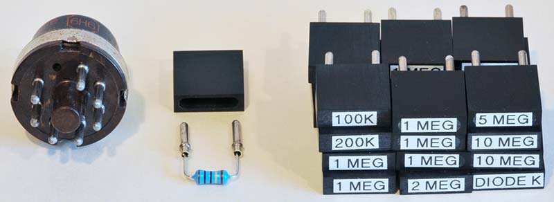
The plug is no longer manufactured. No direct commercial replacement exists. The following options are available, in order of fidelity:
Table 12 — The plug is no longer manufactured. No direct commercial replacement exists. The following options are available, in order of fidelity
| Option | Fidelity | Effort | Cost |
|---|---|---|---|
| Source NOS plugs with the machine | Perfect | Zero (if available) | Included in purchase |
| Harvest from a parts EC-1 | Perfect | Low | Varies |
| Machine reproduction from Delrin rod | Excellent | High (lathe/mill required) | $5–10 per plug in materials |
| Harvest pins from NOS octal tube sockets | Good | Medium | ~$0.50 per plug |
| Direct wire (no plug body — component leads into jacks) | Functional | Very low | Negligible |
| 3D-print body + press-in pins | Good | Medium (FDM printer required) | ~$1 per plug |
7.5.3 Machined Reproduction Plugs
The Nuts & Volts restoration (May 2016) documents machining reproduction plugs from Delrin stock. Key dimensions based on the original phenolic plugs:
Table 13 — The Nuts & Volts restoration (May 2016) documents machining reproduction plugs from Delrin stock. Key dimensions based on the original phenolic plugs
| Dimension | Value | Notes |
|---|---|---|
| Body width | ~0.75” | Overall width across the plug |
| Body height | ~0.60” | Top of body to pin base |
| Body depth | ~0.35” | Front-to-back |
| Pin spacing | ~0.280” (7.1 mm) | Center-to-center |
| Pin diameter | ~0.050” (1.27 mm) | Match original stiff-wire pins |
| Pin protrusion below body | ~0.40” | Depth of socket engagement |
Delrin (acetal resin) is preferred over other plastics: it machines cleanly, is dimensionally stable, and has high dielectric strength (400 V/mil) — adequate for the ±60 V signals. The pins can be cut from 0.050” diameter brass rod (K&S Engineering #8160 or equivalent) and pressed into drilled holes in the Delrin body with cyanoacrylate adhesive.
7.5.4 3D-Printed Reproduction Plugs
A printed plug body is faster to produce than a machined one but requires appropriate material selection:
- Material: PETG or ABS preferred over PLA. PLA softens at 60°C; the EC-1 chassis interior reaches 45–55°C in operation. PETG withstands 80°C continuously.
- Print resolution: 0.1 mm layer height maximum; the pin holes must be within ±0.1 mm of nominal to avoid rocking in the socket.
- Pin installation: Same 0.050” brass rod as machined option.
- Post-processing: Light sanding of the socket-mating surfaces to eliminate layer lines that would cause poor retention.
A printable parametric model can be authored in OpenSCAD from the dimensions above. The pin holes should be undersize by 0.1 mm and reamed to final size with a 1.27 mm drill bit.
7.5.5 Component Values for the Plug Library
The plug-in components serve as the programming resistors and capacitors for each problem setup. A comprehensive working library:
Table 14 — The plug-in components serve as the programming resistors and capacitors for each problem setup. A comprehensive working library
| Value | Type | Plug count recommended | Voltage rating |
|---|---|---|---|
| 100 kΩ | Resistor, 1% metal film, 1/2 W | 20 | Standard (≥50 V) |
| 200 kΩ | Resistor, 1%, 1/2 W | 10 | Standard |
| 500 kΩ | Resistor, 1%, 1/2 W | 10 | Standard |
| 1 MΩ | Resistor, 1%, 1/2 W | 20 | Standard |
| 2 MΩ | Resistor, 1%, 1/2 W | 10 | Standard |
| 5 MΩ | Resistor, 1%, 1/2 W | 5 | Standard |
| 10 MΩ | Resistor, 1%, 1/2 W | 5 | Standard |
| 0.1 µF | Capacitor, film, 630 V | 10 | Must be 630 V |
| 1.0 µF | Capacitor, film, 630 V | 10 | Must be 630 V |
Note — Resistors in the plug library see up to 60 V across them when at the summing junction; 1/2 W metal-film parts rated 200 V or higher are appropriate. Capacitors in integrator feedback positions see the full amplifier output swing (up to ±60 V peak = 120 V peak-to-peak). The 630 V rating provides a factor of 5 safety margin. Standard 50 V or 100 V capacitors must not be used in integrator feedback.
7.5.6 Meter and Switch Hardware
The EC-1’s built-in meter movement is a 50-0-50 µA d’Arsonval galvanometer with a center-zero scale. These are still produced by Sifam Tinsley (UK) and stocked by several analog instrument suppliers. A direct replacement (Sifam Tinsley PM8-50µA or equivalent) is available for ~$35 if the original mechanism is damaged.
The three-position mode switch (IC / OPERATE / RESET) is a heavy-duty rotary wafer switch. Direct replacements for the specific Heathkit part are not available; a functionally equivalent three-position rotary switch with the appropriate contact configuration can be sourced from Grayhill (series 56) or CK Components for $8–$15.
7.6 Safety & Reversibility — Keeping the Restoration Original
7.6.1 The Case for Reversibility
An EC-1 in original, unmodified working condition is historically significant. Heathkit produced approximately 5,000 to 10,000 EC-1 units over a decade; working examples are uncommon. The Nuts & Volts restoration article notes that even machines purchased for as little as $420 represent a meaningful slice of 1960s computing history. Future museum curators, collectors, and scholars will be better served by a machine that can be returned to its exact original state.
Every modification described in this volume is therefore designed to be:
- External — connected only to the front-panel binding posts, never to the internal wiring.
- Non-destructive — nothing drilled, soldered inside, or altered on the original PCB or chassis.
- Documented — all interface boards, attenuator networks, and bench-supply connections are described in a restoration log maintained alongside the machine.
Danger — Never drill new holes in the front panel or chassis for any purpose. The front-panel silk screening is irreplaceable; damage to it cannot be undone. All external connections must use existing binding posts.
7.6.2 Modification Risk Matrix
Table 15 — 6.2 Modification Risk Matrix
| Modification | Reversibility | Risk to Original | Recommended? |
|---|---|---|---|
| Patch cords (modern banana) | Fully reversible | None | Yes |
| 10× oscilloscope probe to output jacks | Fully reversible | None | Yes |
| Attenuator board (external) | Fully reversible | None | Yes |
| USB-DAQ connected via attenuator | Fully reversible | None | Yes |
| External bench supply to B+ binding posts (if exposed) | Reversible | Low, if current-limited | With caution |
| Solid-state daughter board (tube socket) | Reversible if original tubes retained | Medium (socket pins may wear) | With original tubes retained |
| New balance pots (internal) | Partially reversible | Low (desoldering) | Acceptable per Vol 3 |
| New electrolytics (internal) | Partially reversible | Low | Standard restoration practice |
| Drilling chassis for new connectors | Irreversible | High | No |
| Painting original aluminum front panel | Irreversible | High | No |
7.6.3 Isolation Protocol Before Internal Access
Danger — The EC-1 contains lethal voltages: +300 V on the B+ bus, −150 V on the negative rail, and 120 VAC on the primary wiring. Before opening the chassis for any reason:
- Switch the FILAMENT / HIGH VOLTAGE switch to off and the main power switch to off.
- Unplug the AC line cord.
- Wait at least 5 minutes for the filter capacitors (up to 50 µF at 350 V) to discharge through the bleeder resistors.
- Measure the B+ rail with an insulated-probe DMM set to the 600 V DC range. Confirm voltage below 10 V before touching any internal component.
- Work with one hand; keep the other hand away from the chassis.
7.6.4 Documentation Standards
Every external interface built for the EC-1 should be documented with:
- A schematic or block diagram of the interface.
- A BOM with part numbers and purchase dates.
- A calibration record (input/output voltages at a minimum of three test points).
- Photographs of the completed interface board and its connection to the EC-1.
- A reversibility statement explaining exactly how the interface is removed.
Store this documentation alongside the EC-1 manuals. If the machine is ever sold or donated, the documentation transfers with it.
7.6.5 Calibration Record Template
Table 16 — 6.5 Calibration Record Template
| Date | Interface | Test Point | Applied Voltage | Measured Output | Ratio | Technician |
|---|---|---|---|---|---|---|
| — | Attenuator Ch1 | EC-1 Amp 1 out | +30.00 V | +2.498 V | 12.01 | — |
| — | Attenuator Ch1 | EC-1 Amp 1 out | −30.00 V | −2.502 V | 11.99 | — |
| — | Attenuator Ch2 | EC-1 Amp 2 out | +60.00 V | +4.997 V | 12.01 | — |
Ideal ratio is 12.000; values within ±0.5% indicate a well-matched divider. Values outside ±1% suggest a resistor out of tolerance or a solder joint issue.
7.6.6 Chassis Photo Reference — Inside the Restored EC-1
The photograph below shows the internal layout of a restored EC-1 chassis, illustrating the five bus bars, the tube complement, and the power supply section. All external interface connections must be made at the front panel binding posts, not at any point visible in this photograph.
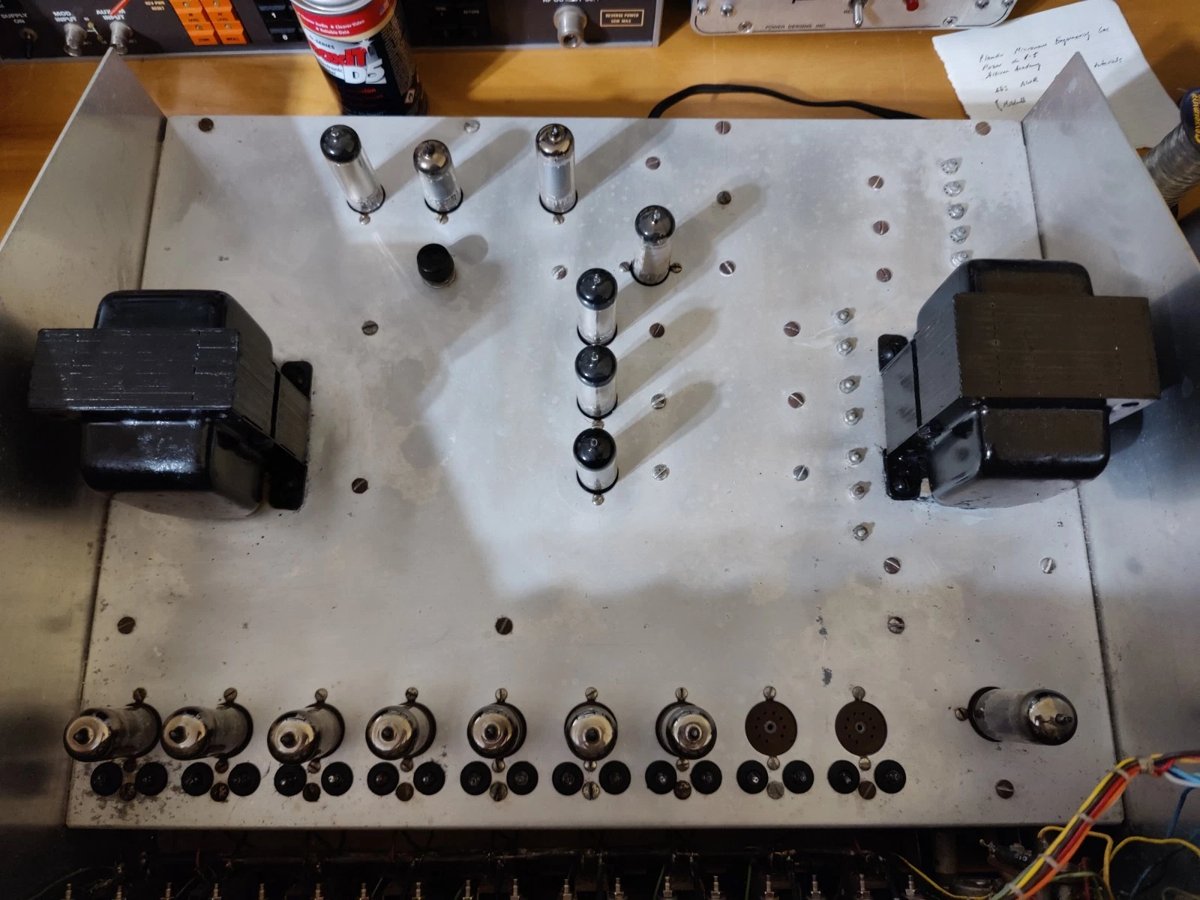
The bus bars that distribute B+, B−, and heater voltages run horizontally across the rear of the chassis. They are uninsulated and present a lethal shock hazard whenever the chassis is energized. The safety isolation protocol in §6.3 must be followed before this area is approached.
7.6.7 Long-Term Storage
If the EC-1 is to be stored for more than six months:
- Remove tubes and store individually in labeled cardboard boxes (original tube boxes are ideal). Tube storage prevents heater filament sag and avoids vibration-induced cathode damage.
- Leave the front panel switches in their normal operating positions (or mid-travel) to avoid switch contact impression.
- Store at 40–70°F, below 60% relative humidity. Electrolytic capacitors that have been recently reformed (< 2 years) will tolerate up to 24 months of unformed storage without significant degradation; beyond that, the forming procedure (§4.7) should be repeated before powering up.
- Keep the operator and assembly manuals inside the chassis case, or in an acid-free archival envelope attached to the machine.
Tip — Photograph the front-panel patch state of any problem setup before disassembly. The EC-1’s “program” exists only in its patch cords, resistor plugs, and potentiometer settings. A photograph is the only way to restore it exactly.
7.7 Appendix A — Quick Reference: Modern Interface Connections
┌──────────────────────────────────────────────────────────────────┐
│          EC-1 EXTERNAL INTERFACE QUICK-REFERENCE CARD            │
├─────────────────┬────────────────────────────────────────────────┤
│ SIGNAL POINT    │ SAFE EXTERNAL CONNECTION METHOD                │
├─────────────────┼────────────────────────────────────────────────┤
│ Amp 1–9 output  │ 10× scope probe direct; or attenuator board    │
│ (±60 V, red)    │ (110k/10k divider + OPA2134 buffer → ADC)     │
├─────────────────┼────────────────────────────────────────────────┤
│ Signal ground   │ Black binding post; tie to instrument ground   │
│ (0 V, black)    │ ONCE. Do not create ground loops.             │
├─────────────────┼────────────────────────────────────────────────┤
│ Coeff pot wiper │ Connect to amp input via problem resistor plug │
│ (0 to ±60 V)   │ No direct external instrument connection       │
├─────────────────┼────────────────────────────────────────────────┤
│ IC supplies     │ Connect to amplifier IC input jack via patch   │
│ (+100 V, red)   │ cord only. Do NOT connect external equipment. │
├─────────────────┼────────────────────────────────────────────────┤
│ Oscilloscope    │ CH1 ← X-axis variable; CH2 ← Y-axis variable  │
│ X-Y output jacks│ Scope set to DC coupling; X-Y mode; 10 V/div  │
│                 │ (×10 probe) or 20 V/div (÷2 at scope input)   │
└─────────────────┴────────────────────────────────────────────────┘

NEVER connect to: B+ bus bar, B− rail, heater wiring, transformer
taps, or any point inside the chassis while power is applied.
7.8 Appendix B — Troubleshooting External Interface Issues
Table 17 — Appendix B — Troubleshooting External Interface Issues
| Symptom | Probable Cause | Diagnosis | Remedy |
|---|---|---|---|
| ADC reads zero despite EC-1 running | Attenuator output open | Measure at buffer op-amp output with DMM | Check solder joints; verify op-amp supply |
| ADC reads correct voltage but noisy (~100 mV RMS) | Ground loop between EC-1 and DAQ | Lift DAQ ground at one end; use differential input | Use isolated USB-DAQ or add common-mode choke |
| Scope display shows 60 Hz hum on all channels | EC-1 heater coupling or scope probe ground loop | Reduce probe ground lead length; try battery-powered scope | Improve heater supply isolation; see §4.5 |
| Attenuator output clips at +5 V with EC-1 at +40 V | Buffer op-amp supply too low or resistor wrong | Measure R1 and R2 in-circuit with DMM (power off) | Verify R1 = 110 kΩ ±1%; check supply voltage to op-amp |
| Logged data shows step discontinuities | USB-DAQ sample rate too slow for repetitive mode | Increase sample rate; check USB bus load | Reduce sample rate or use dedicated scope |
| External bench supply trips current limit | Short in B+ connection or unreformed capacitor | Disconnect EC-1; measure resistance to GND | Increase current limit gradually; reform caps per §4.7 |
| Attenuator reads −2 V offset with no EC-1 signal | Op-amp input bias or divider unbalanced | Short attenuator input to GND; observe offset | Adjust offset trim on buffer op-amp; check R2 value |
Volume 7 of 8 — Heathkit EC-1 Educational Analog Computer Reference Series.
See Vol 2 for op-amp circuit theory and power-supply detail; Vol 3 for patch panel and computing elements; Vol 4 for restoration procedure; Vol 5 for programming and problem setups; Vol 6 for sample programs.
Comments (0)